Controlled formation of metallic nanowires via Au nanoparticle ac trapping
Abstract
Applying ac voltages, we trapped gold nanoparticles between microfabricated electrodes under well-defined conditions. We demonstrate that the nanoparticles can be controllably fused together to form homogeneous gold nanowires with pre-defined diameters and conductance values. Whereas electromigration is known to form a gap when a dc voltage is applied, this ac technique achieves the opposite, thereby completing the toolkit for the fabrication of nanoscale junctions.
pacs:
73.23.-b, 73.40.Jn, 73.63.-b, 73.63.Rt, 81.07.-b, 81.07.Lk, 81.16.Rf1 Introduction
Novel nanometer-scale electronic systems have been extensively developed during the last few years. For example, field-effect transistors made from carbon nanotubes [1] and organic molecules [2, 3] are being designed to constitute alternative routes to Si-based technology. Molecular electronics in particular combines several advantages: nanometer-scale size, flexibility of chemical synthesis and discrete energy levels. These aspects make molecules appear as promising building blocks for ultimate nano-electronics [4]. However, a key challenge within this size range remains the control of the connection between a few molecules and macroscopic current and voltage leads [5]. This requires the fabrication of contacts down to the size of a few nanometers. Electron-beam lithography can presently only hardly reach sub- nm resolution, or under very specific conditions[6, 7, 8]. Thus, new techniques need to be developed to produce nano-scale contacts. Among others, one philosophy is to start from e-beam prefabricated micro-electrodes and decrease the gap in a second step, for example via electrodeposition[9]. A promising method is to close the gap by metallic nanoparticles, used as intermediates, linking the molecules to the electrodes [10, 11, 12, 13, 14]. Hence, there is a need for the precise positioning of nanoparticles within larger structures.
A simple and controllable method to position nanoparticles is reported here. It consists of aligning and contacting colloids by means of dielectrophoresis (ac trapping) [15, 16, 17]. This technique has previously been used to manipulate a variety of micrometer- and nanometer-size objects including biopolymers [18, 19], cells [20] and metallic colloids [21, 22, 23, 10, 24, 25]. However, a systematic approach is still lacking. This is in particular true concerning the assembly of metallic particles in sub-micrometer gap sizes. In the present work, the process of ac trapping nanoparticles with diameters in between nm and nm into gaps of widths ranging from nm to nm has been investigated. Remarkably, the technique enables one to form continuous nanowires of tunable diameter between microfabricated electrodes. This process can be initiated by choosing the proper ac voltage and series impedance.
2 Experimental
Pairs of planar, tip-shaped gold (Au) electrodes facing each other were patterned on a Si/SiO2 substrate using conventional UV and electron-beam lithography (EBL). Before each fabrication step, the substrate was cleaned in acetone, followed by isopropanol and was finally exposed to an oxygen plasma for min. After resist spinning, exposure and development, a nm thick adhesion layer of Ti was deposited prior to the evaporation of a nm Au layer. The tips of the electrodes pairs were separated by a gap typically ranging between and nm. Using an angle evaporation technique, the gap size can be reduced to less than nm, however with a relatively small yield ().
Colloidal solutions of charge-stabilised Au particles were prepared following the method of Turkevich et al. [26]. A mM solution of was reduced with aqueous citric acid at boiling temperature. This resulted in nearly monodisperse charge-stabilised Au colloids with a diameter between nm and nm, depending on the reducing agent concentration. Using these charge-stabilised Au colloids as the starting material, we have also prepared alkane-thiol encapsulated Au colloids following the method of Huang et al. [27]. For subsequent experiments, the encapsulated colloidal particles were dissolved in a mixture of hexane and dichloromethane.
Trapping of the Au nanoparticles was performed via dielectrophoresis (DEP) by applying an ac electric field between the two electrodes. The dielectrophoretic force acting on a homogeneous, isotropic particle of radius is proportional to the gradient of the electric field amplitude squared and reads [17]:
where denotes the real part. The effective polarizability of the particle in the medium is expressed by the relative permittivities of the particle and the medium . This force typically ranges from pN to pN [16, 17].
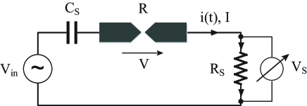
A circuit diagram of our setup is sketched in Figure 1. The scheme includes a series capacitor and a series resistor , which constitute a total series impedance . The capacitor was placed in the circuit to filter out any dc component and to avoid electrochemical processes or electromigration [28]. It also prevented further effects due to, for instance, the electrophoretic mobility of the ionic solution, which can influence the motion of the suspended nanoparticles. To measure the time-dependence of the current, , we recorded the voltage drop over . For this, both a time-averaging lock-in amplifier and a fast digital oscilloscope were used. The lock-in amplifier continuously monitored the trapping process with a time-resolution of ms. In contrast, the oscilloscope, which provided a much faster time resolution of ns, was adjusted to trigger at the trapping event, when a significant increase of the current amplitude was monitored. In this way we measured the delay time until a particle is trapped and the temporal evolution of the impedance during junction formation. In order to limit the number of parameters in the process, we fixed the frequency of the ac field throughout the trapping experiments to a value of 1 MHz. This allowed the manipulation of nanoparticles with diameters ranging between nm and nm at concentrations of order mL-1. Typical values for the total input voltage and the series resistor were V and , respectively. Throughout this paper, the symbols , , and refer to the RMS values of the current, voltage, resistance and dissipation at (in) the junction, respectively. During the trapping process, they are time dependent. Their final values, once the trapping is completed, are denoted by , , and , respectively.
3 Results and discussion
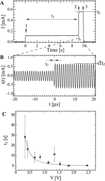
We explored various types of colloids with a main focus on charge-stabilised Au colloids with a diameter of nm. To investigate the trapping process in detail, the current through junctions was measured during and after the trapping of these specific particles. All samples were prepared following the same procedure. Figure 2A shows a typical lock-in measurement of the current flowing through a junction during trapping. First, a colloidal solution droplet was deposited on the device (). Next, an ac trapping voltage was applied at to attract the nanoparticles to the junction. This gave rise to a detectable leakage current through the solution (arrow 1). After the duration of typically a few seconds to one minute, a large current increase was suddenly observed (arrow 2). This event signals the formation of a conducting bridge within the gap due to the trapping of individual nanoparticles. The conductance jump takes place when the last nanoparticle gets trapped and completes the closing of the gap. After this increase, the current remained constant and finally, the input voltage was set to zero (arrow 3). We note that in a few particular cases the current did not increase in a single step, but rather displayed multiple steps, suggesting the formation of a few conducting bridges in parallel. Figure 2B shows a typical oscilloscope trace of , set up to trigger exactly at the current increase (arrow 2, Figure 2A). We see that the junction changes its resistance typically within s. Figure 2C shows the dependence of the average trapping time on the voltage over the junction (for ). The trapping time roughly scales with the inverse of the voltage squared , which agrees with the expectation for a driven particle movement impeded by viscous friction. In that case the velocity scales with the driving force which is, according to the expression for the dielectrophoretic force, proportional to the electric field squared, and hence to the voltage squared.
After each trapping experiment, scanning-electron microscopy (SEM) inspection of the samples revealed that in cases the junctions showed no sign of breakdown. Figure 3 reports a set of representative results. First, we focus on Figures 3A and 3B. Here, nanoparticles with a relatively large diameter of nm were trapped into 500 nm large gaps. The trapping conditions for both cases were identical, except for the applied voltage : V in case A and V in case B. We clearly observe a larger number of trapped particles in A than in B. This illustrates that one can tune the number of nanoparticles bridging the gap by adjusting the trapping voltage. The electric field required for optimal trapping amounts to about V/m. In Figure 3B, a well-ordered chain of nanoparticles was formed with a junction resistance of only . This is surprising and indicates that after the nanoparticles were trapped, a second, ‘anchoring’ process took place. During anchoring, the colloids become physically and electrically connected, leading to a low final resistance. Figure 3C shows a device in which even smaller particles, i.e. nm, were trapped, with an applied voltage V. Remarkably, the individual colloids are not distinguishable any longer. Instead of building a chain, as in Figure 3B, the particles have fused together forming a wire with a well defined diameter. The final resistance of this wire is comparatively low, i.e. . Figure 3 shows that the anchoring process can lead to the formation of two distinct structures: chains or wires. Below, we will discuss this phenomenon in more detail. Finally, in Figure 3D and E, we show examples of junctions with relatively large final resistances in the M range. In Figure 3D, a single nanoparticle ( nm) was trapped. In contrast to Figures 3A-D where charge-stabilised colloids were used, Figure 3E shows a typical result for the trapping of dodecanethiol ()-functionalized nanoparticles of nm diameter within a nm gap. Unlike the former cases, devices made with functionalized particles never displayed fusing and the resistance values were always large ().
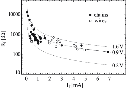
In cases of the successful trapping experiments with nm diameter charge-stabilised nanoparticles, the final junction resistance was much larger than M. This indicates that no metallic contact was established between the nanoparticles and the electrodes. An overview of the rest of the data set ( experiments) is given in Figure 4. Here, we plot the final device resistance as a function of the current , both measured at the end of the trapping and anchoring process. There is quite some scatter in the final resistance of the devices. Nevertheless, the data set is confined between a lower and an upper bound given by the voltage . More precisely, the voltage over the junction always lies in between V and V, as indicated by the dotted lines, a typical value being V. The lower bound in Figure 4 is related to the trapping process: if the electric field is too small, trapping does not take place. In contrast, a voltage that is too large leads to sample destruction after trapping as evidenced by ‘burnt’ electrodes which are modified on a macroscopic scale. This breakdown process is likely related to a thermal run-away by excessive Joule heating as reported in electromigration experiments on nanojunctions [29, 30, 31]. The open and solid data points in Figure 4 relate to two different kinds of junctions. The solid dots refer to junctions in which the nanoparticles formed chains during the trapping process (cf. Figure 3B), whereas the open dots relate to wire formation (cf. Figure 3C). It appears that the two subsets group together in Figure 4, despite the clear scatter. Hence, Figure 4 forms a good basis to discuss about the possible processes behind anchoring, chain and wire formation, as well as device breakdown.
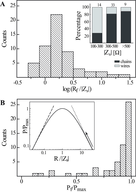
We first focus on the moment when a set of nanoparticles is being trapped in the junction at . These particles experience a large electric field in the gap region V/m, which induces a dipole in each of them. Consequently, the dipole-dipole interaction between the particles becomes significant, tending to line up the particles in the junction. This explains the preference for the initial chain formation. At that point, the charge-stabilised particles are not yet interconnected, so that the whole voltage drops over the tiny gaps (1 nm) between the particles. This has two consequences. First, the electric field is much more localised than before chain formation. Hence, the range of the DEP force is decreased, leading to a much smaller trapping probability for left-over particles in the solution. In this way, DEP is self-limiting. Second, the field over the gaps between the individual colloids tend to become very high, V/m. At such fields, surface diffusion of Au atoms is enhanced in the direction of the gap and can lead to the formation of narrow Au bridges between the nanoparticles [32, 33]. If no connections are formed, a device will have a high final resistance ( 1 M), as observed in of our junctions made with charge-stabilised particles. As mentioned above, junctions prepared with alkanethiol-covered particles always yielded high resistance values, suggesting that the alkanethiol shell protects the colloids against field-driven atomic migration. However, in most devices with charge-stabilised particles, the particles were interconnected and the resistance of the devices dropped dramatically. One may wonder what determines the final value of these junctions. To address this point, we refer to Figure 5A, where a histogram of is plotted. This graph describes the probability distribution of the ratio of to the total series impedance . We find that is typically of the same order of magnitude as . The histogram features a clear peak with a maximum around a ratio of , corresponding to . In the inset of Figure 5A, we show a stacked bar plot of the percentage of chains (dark) and wires (light) for three ranges of . Interestingly, chains are more common for higher , while wires are mostly found for lower . Figure 5A indicates that we can tune (at least roughly) the device properties via the series impedance.
To understand this, we bring forward a possible model of wire formation. We first note that a change in shape from chain to wire leads to a decrease of the total surface energy. Hence, we expect that surface tension is the effective driving force for the fusing process. Also, in order to transform a chain of spherical particles into a rod-like wire, a considerable diffusion of Au atoms is needed. Since diffusion is an activated process, an increase of the junction temperature by Joule heating will clearly facilitate wire formation. Before fusing, and the junction is voltage-biased with the power dissipated over the junction given by . Once atomic diffusion sets in and the gaps start to fill up, the resistance decreases and consequently the dissipation increases. If the applied voltage is too large, this can lead to a thermal run-away and sample breakdown. However, the series impedance also has an effect on . It can self-limit the thermal run-away process for moderate . To see this, we note that the junction would be current-driven in the opposite regime . In that case, the local dissipation is given by and decreases with decreasing , thus limiting the fusion process. The full dependence of on is shown in the inset of Figure 5B. There is a maximum power at . The dashed and dotted lines indicate the dissipation in the limiting cases of effectively current-biased and voltage-biased junctions, respectively. Based on this consideration, we expect the process to stop when where the dissipation reaches its maximum. Hence, the final dissipation , measured at the end of successful junction formation, should be close to . In Figure 5B, we display a histogram of for all data points in Figure 4. For the vast majority of our devices, Figure 5B shows that , as anticipated. Because the final resistance is generally a bit larger than (Figure 5A), we infer that the process tends to stops to the right of the maximum in the inset of Figure 5B.
Relating the junction temperature to the power is not straightforward, but it can be stated that is related to the volume power density . If we assume for simplicity that only the junction cross-section changes during wire formation, but not its length , we have . Because one may also write . Hence, in the beginning, when and , the power density is constant, even if increases due to the thermally driven diffusion of Au atoms. This homogenization process can therefore go on at constant temperature until the assumption is no longer valid. Then, and hence will decrease, limiting atomic diffusion. This picture suggests that the homogenisation process can proceed further for small as compared to large . It therefore becomes understandable why wire-like devices appear for small , whereas chain-like ones appear for large , consistent with the inset of Figure 5A.
In the previous discussion, electromigration was ignored, since it does not occur for the ac current densities we apply [28]. In fact, electromigration at similar dc current densities leads to gap formation [2, 3, 31], which is the opposite effect compared to the new ‘gap-closing’ process that we report here. Interestingly, the series impedance and Joule heating play a similar role in electromigration experiments as in the work presented here [31]. We speculate that repeated gap formation and closing should be possible by using ac and dc voltages, alternately.
4 Conclusions
We demonstrate a simple method to control the formation of metallic nanowires and chains of desired length and diameter. It is based on the dielectrophoretic trapping of nanoparticles. We point out the relevance of two processes: the trapping and the subsequent anchoring of the particles between the electrodes. By choosing a proper series impedance, one can tune the final resistance and appearance of a junction: lower series impedances favor wire formation, whereas higher series impedances result in chains. The nanostructures produced are promising elements in the framework of nanoelectronics. For instance, they can be used to contact nanometer-size building blocks, possibly in combination with dc electromigration. Using this approach, it may become possible to fine tune nanogaps in electromigration devices, which is of high interest to molecular electronics.
References
References
- [1] S.J. Wind, J. Appenzeller, R. Martel, V. Derycke, and Ph. Avouris. Vertical scaling of carbon nanotube field-effect transistors using top gate electrodes. Appl. Phys. Lett., 80:3817–3819, 2002.
- [2] W. Liang, M.P. Shores, M. Bockrath, J.R. Long, and H. Park. Kondo resonance in a single-molecule transistor. Nature, 417:725–729, 2002.
- [3] H.S.J. van der Zant, Y.-V. Kervennic, M. Poot, K. O Neill, Z. de Groot, J.M. Thijssen, H.B. Heersche, N. Stuhr-Hansen, T. Bjørnholm, D. Vanmaekelbergh, C.A. van Walreed, and L.W. Jenneskens. Molecular three-terminal devices: fabrication and measurements. Faraday Discuss., 131:347–356, 2006.
- [4] J.R. Heath and M.A. Ratner. Physics Today, 56:43–49, 2003.
- [5] K.W. Hipps. Science, 294:536–537, 2003.
- [6] K. R. V. Subramanian, M. S. M. Saifullah, E. Tapley, D.-J. Kang, M. E. Welland, and M. Butler. Direct writing of ZrO2 on a sub-10 nm scale using an electron beam. Nanotechnology, 15:158–162, 2004.
- [7] K. Liu, Ph. Avouris, J. Bucchignano, R. Martel, and S. Sun. Simple fabrication scheme for sub-10 nm electrode gaps using electronbeam lithography. Appl. Phys. Lett., 80:865–867, 2002.
- [8] P. Steinmann and J. M. R. Weaver. Nanometer-scale gaps between metallic electrodes fabricated using a statistical alignment technique. Appl. Phys. Lett., 86:063104, 2005.
- [9] A.F. Morpurgo, C.M. Marcus, and D.B. Robinson. Controlled fabrication of metallic electrodes with atomic separation. Appl. Phys. Lett., 74:2084–2086, 1999.
- [10] AS.I. Khondaker and Z. Yao. Appl. Phys. Lett., 81:4613–4615, 2002.
- [11] T. Dadosh, Y. Gordin, R. Krahne, I. Khivrich, D. Mahalu, V. Frydman, J. Sperling, A. Yacoby, and I. Bar-Joseph. Measurement of the conductance of single conjugated molecules. Nature, 436:677–680, 2005.
- [12] D. P. Long, C. H. Patterson, M. H. Moore, D. S. Seferos, G. C. Bazan, and J. G. Kushmerick. Magnetic directed assembly of molecular junctions. Appl. Phys. Lett., 86:153105, 2005.
- [13] J. Liao, L. Bernard, M. Calame, and C. Schönenberger. Reversible formation of molecular junctions in twodimensional nanoparticle arrays. Adv. Mater., 18:2444–2447, 2006.
- [14] C. Xu, H. van Zalinge, J.L. Pearson, A. Glidle, J.M. Cooper, D.R.S. Cumming, W. Haiss, J.L. Yao, D.J. Schiffrin, M. Proupín-Pérez, R. Cosstick, and R.J. Nichols. A combined top-down bottom-up approach for introducing nanoparticle networks into nanoelectrode gaps. Nanotechnology, 17:3333–3339, 2006.
- [15] H.A. Pohl. Dielectrophoresis. Cambridge University Press, 1978.
- [16] T.B. Jones. Electromechanics of particles. Cambridge University Press, 1995.
- [17] H. Morgan and N.G.Green. AC electrokinetics. Research Studies Press; Baldock, England., 2003.
- [18] M. Washizu, S. Suzuki, O. Kurosawa, T. Nishizaka, and T. Shinoara. IEEE Trans. Ind. Appl., 30:835–843, 1994.
- [19] F. Dewarrat, M. Calame, and C. Schönenberger. Single Molecules, 3:189–193, 2002.
- [20] R. Pethig and G.H. Marx. Trends in Biotech., 15:426–432, 1997.
- [21] A. Bezryadin, C. Dekker, and G. Schmid. Electrostatic trapping of single conducting nanoparticles between nanoelectrodes. Appl. Phys. Lett., 71:1273–1275, 1997.
- [22] K.D. Hermanson, S.O. Lumsdon, J.P. Williams, E.W. Kaler, and O.D. Veley. Science, 294:1082–1086, 2001.
- [23] I. Amlani, A.M. Rawlett, L.A. Nagahara, and R.K. Tsui. Appl. Phys. Lett., 80:2761–2763, 2002.
- [24] R. Kretschmer and W. Fritzsche. Pearl chain formation of nanoparticles in microelectrode gaps by dielectrophoresis. Langmuir, 20:11797–11801, 2004.
- [25] S. O. Lumsdon and D. M. Scott. Assembly of colloidal particles into microwires using an alternating electric field. Langmuir, 21:4874–4880, 2005.
- [26] J. Turkevich, P.C. Stevenson, and J. Hillier. Discuss. Faraday Soc., 11:55–75, 1951.
- [27] S. Huang, G. Tsutsui, H. Sakaue, S. Shingubara, and T. Takahagi. J. Vac. Sci. Technol. B, 19:115–120, 2001.
- [28] K.P. Rodbell, A.J. Castellano, and R.I Kaufman. Ac electromigration (10mhz-1mhz) in Al metallization. AIP Conf. Proc., 418:212–223, 1998.
- [29] C. Durkan, M. A. Schneider, and M. E. Welland. Analysis of failure mechanisms in electrically stressed Au nanowires. J. Appl. Phys., 86:1280–1286, 1999.
- [30] M.F. Lambert, M.F. Goffman, J.P. Bourgoin, and P. Hesto. Nanotechnology, 14:772–777, 2003.
- [31] M. L. Trouwborst, S. J. van der Molen, and B. J. van Wees. The role of joule heating in the formation of nanogaps by electromigration. Journal of Applied Physics, 99:114316, 2006.
- [32] T.T. Tsong. Effects of electric field in atomic manipulations. Physical Review B, 44:13703–13710, 1991.
- [33] J. Méndez, J. Gómez-Herrero, J.I. Pascual, J.J. Sáenz, J.M. Soler, and A.M. Baró. Diffusion of atoms on Au(111) by the electric field gradient in scanning tunneling microscopy. J. Vac. Sci. Technol. B, 14:1145–1148, 1996.


