Electronic address: ]okapon@ornl.gov
Nonequilibrium transport and optical properties of model metal–Mott-insulator–metal heterostructures
Abstract
Electronic properties of heterostructures in which a finite number of Mott-insulator layers are sandwiched by semi-infinite metallic leads are investigated by using the dynamical-mean-field method combined with the Keldysh Green’s function technique to account for the finite bias voltage between the leads. Current across the junction is computed as a function of bias voltage. Electron spectral functions in the interacting region are shown to evolve by an applied bias voltage. This effect is measurable by photoemission spectroscopy and scanning tunneling microscopy. Further predictions are made for the optical conductivity under a bias voltage as a possible tool to detect a deformed density of states. A general discussion of correlated-electron based heterostructures and future prospect is given.
pacs:
73.20.-r,73.40.Rw,72.90.+yI Introduction
Correlated-electron materials including transition-metal oxides have provided the basis for a variety of properties such as high- superconductivity in cuprates and colossal-magnetoresistance (CMR) in manganites.Imada98 Therefore it is anticipated that these materials will become the core of future electronic devices. For this purpose, the fabrication and characterization of interfaces including correlated-electron materials are of fundamental importance. In recent years, we have seen a tremendous amount of work on such heterostructures. Developments in thin film growth techniqueKawasaki94 enable us to fabricate “digital” heterostructures out of correlated materials with atomic resolution,Ahn99 ; Izumi01 ; Gariglio02 ; Ohtomo02 and developments in scanning microscopyBatson93 ; Muller93 ; Browning93 enable us to characterize the physical properties including conduction band electron distribution of the heterostructures.Ohtomo02 Furthermore, fabrication of practical devices has already started. This includes Josephson junctionBozovic03 ; Bozovic04 and tunneling magnetoresistance (TMR) junctionsSun96 ; Bowen03 with device characteristics that remain to be optimized.
These experimental developments stimulated a great deal of theoretical research on correlated-electron heterostructures.Freericks04 ; Okamoto04a ; Okamoto04b ; Oka05 ; Lee06 ; Kancharla06 So far, most work has focused on the ground-state properties such as spectral function, charge density distribution, and linear conductance. As metal–semiconductor (or band insulator)–metal heterostructures provide one of the fundamental building brocks of current electronics,Esaki58 ; Josephson74 ; Giaever74 establishing the electric properties of correlated heterostructures is of great importance. Detailed analysis of the transport properties of correlated heterostructures including current-voltage characteristics is directly relevant to device applications.Bozovic03 ; Bozovic04 ; Sun96 ; Bowen03 However, this area remains largely unexplored.
In this paper, we investigate the properties of heterojunctions consisting of a correlated insulator embedded in semi-infinite metallic leads. In particular, we focus on the steady state with an applied bias voltage between the leads. The effect of strong correlations is treated by using the dynamical-mean-field theory (DMFT)Georges96 combined with the Keldysh Green’s function techniqueKeldysh65 to account for the finite bias voltage. We present current vs voltage characteristics of the junctions, position-dependent spectral functions, and optical conductivity spectra, and discuss how the transport properties of heterostructures are affected by correlations.
II Model and formalism
II.1 Model
We consider electrons moving on a cubic lattice with lattice constant (=1) and discrete translational invariance in the plane. Thus each site is labeled by with . A Hubbard-type interaction is introduced at a number of layers (sample ) located from to , and noninteracting leads are located at (lead ) and (lead ). We consider the nearest-neighbor transfer () of electrons in the sample (lead ), the hybridization between the sample and lead , and the layer-dependent potential (see Fig. 1). Thus the Hamiltonian for this system is written as with
| (1) |
and
| (2) | |||||
| (3) | |||||
| (4) |
with and describing the interacting region and lead , respectively, and the hybridization between the sample and the lead . is an electron annihilation operator at position with spin , and . The position in each term is constrained as explained above and is the unit vector .
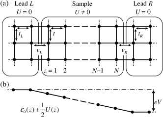
II.2 Layer dynamical-mean-field theory with finite bias voltage
To apply a finite bias voltage, we adiabatically turn on the hybridization and interaction between the leads and the sample.Caroli71 ; Datta Before turning on the hybridization and interactions, the two leads have the chemical potentials and as well as the site potentials and . The potential in the central region varies accordingly. We assume that the two leads are infinitely large and unaffected by the interactions, and thus remain in equilibrium. Under these conditions, the noninteracting leads are integrated out, and the electronic state of the interacting region may be described by the following Green’s function matrices in the in-plane momentum and -axis coordinate representation:
| (5) | |||||
| (6) |
Here, and stand for retarded (advanced) and Keldysh components of the Green’s function matrices, respectively, and . is the noninteracting retarded Green’s function given by and are the retarded and the Keldysh self-energies, respectively, representing the effects of both electron correlation and the hybridization with the leads. The latter part of the self-energy can be obtained from the noninteracting Green’s functions. Thus what must be determined is the self-energy due to correlations.
In order to fix the correlation part of the self-energy, we generalize the layer DMFT.Potthoff99 ; Freericks01 ; Okamoto04b Dynamical-mean-field theory using the Keldysh technique has been applied to solve the bulk correlated-electron model influenced by a time-dependent external field,Schmidt02 ; Freericks06 while our focus is the steady state. In the layer DMFT, the self-energy due to correlations is approximated to be diagonal in layer index and independent of in-plane momentum. Thus the lattice self-energy is written as
| (7) | |||||
where and . is the retarded (advanced) Green’s function of lead projected on the layers adjacent to the interacting region, and
| (8) |
is the Keldysh Green’s function of lead . This function describes the distribution of electrons in terms of the Fermi distribution function with inverse temperature and chemical potential .
In DMFT, the quantum impurity model is introduced as a mathematical tool to compute the electron self-energy. The self-consistency condition of DMFT is closed by identifying the impurity Green’s function with the local part of the lattice Green’s function as
| (9) |
where and . The impurity model at each is characterized by the hybridization function and the nonequilibrium distribution function of electrons (in equilibrium, this is just the Fermi distribution function). The hybridization function represents the intersite virtual transfer of electrons in the form of the effective conduction band coupled to the impurity orbital. This includes intralayer and interlayer couplings and the hybridization between the sample and the leads. As in the equilibrium case,Georges96 the self-consistency condition determining this function is
| (10) |
The nonequilibrium distribution function is fixed by the local Keldysh Green’s function as
| (11) |
Note that in the steady state we are focusing on, there is no net charge flow between the impurity orbital and the effective conduction band, i.e., the impurity model is in local “equilibrium” described by . Therefore, the Keldysh components of the self-energy and the hybridization function are related to the retarded ones by and , respectively. Thus the self-consistency condition of DMFT is closed by Eqs. (10) and (11) with Eq. (9).
The remaining task is to solve the quantum impurity model defined by the hybridization function and the distribution function with the local interaction. For this purpose, we employ the equation-of-motion decoupling (EOM) scheme,Appelbaum69 ; Lacroix81 which has been applied to study the nonequilibrium properties of quantum dotsMeir91 and to solve the quantum impurity models of DMFT in equilibrium.Gros94 ; Jeschke05 ; Zhu04 In the EOM scheme, the retarded self-energy is given by (including spin dependence explicitly as and )
| (12) |
with , and
| (13) |
with and .Zhu04
We pause to make one remark on solving the self-consistency equations. During the computation, we noticed that updating the distribution function directly from Eq. (11) by dividing both sides by does not provide smooth convergency. Instead, we found it more efficient to first rewrite the right hand side of Eq. (11) as and then to update from .
It may be worth pointing out the limitation of the EOM scheme. As discussed in detail by Gros, the EOM scheme does not describe the correct metallic state of the Hubbard model at half filling. Thus, it fails to describe the bulk metal-insulator transition.Gros94 This is because the EOM scheme is essentially a strong coupling expansion, and therefore “Kondo” physics is not fully taken into account. Although some amount of Kondo physics is included by the exchange of electrons between the impurity orbital and the conduction band, it disappears in the particle-hole symmetric case. Therefore, it is favorable to take the on-site interaction larger than the critical value of the bulk Mott transition at half filling. When it is applied to the non-integer filling, the EOM scheme can reproduce the resonance-peak structure at the Fermi level at low temperature.Appelbaum69 ; Lacroix81 However, such Kondo physics is not fully taken into account. Therefore, results become less reliable at temperatures much lower than the characteristic Kondo temperature.
Although it may not be easy, some improvement in the impurity solver of DMFT seems possible. For weak-to-intermediate interaction , generalized iteration perturbation theory (IPT) Kajueter96 ; Schmidt02 seems realistic. But including higher-order perturbation processes in terms of may be necessaryFujii03 because the simple second-order perturbation with respect to does not capture the nonequilibrium Kondo feature when it is applied to the quantum dot problem.Hershfield91 For intermediate-to-strong coupling, the noncrossing approximationPruschke93 may be applicable. However, this method is known to exhibit artificial structure in the spectral function at low temperature.Meir91 Another possibility is to use the recently developed continuous-time quantum Monte Carlo method,Rubtsov05 ; Werner06 which could be applied to a wider range of parameters. This method is formulated on the imaginary time axis assuming the system is in equilibrium. Therefore in order to apply it to the nonequilibrium situation, it is necessary to modify the method to deal with real time (or real frequency).
II.3 Physical quantities
Once self-consistency in the DMFT equations is achieved, one can proceed to compute physical quantities using the “lattice” Green’s functions. Here, we first consider steady-state electric currents. In the steady state with a potential gradient along the direction, the current is uniform in space and time. Therefore one can measure the current through any bond along the direction (the steady current is conserved in the present formalism). Using the Keldysh Green’s function matrix, the electric current per spin and per unit area between the and layers is computed as
| (14) |
Another physical quantity of interest is the optical conductivity which can provide information about the dynamical properties of the system. In order to obtain the optical conductivity, a linear coupling between the current and the vector potential is first introduced according to the Pires-phase approximation as . Then, the expectation value of the current to linear order in is computed using the nonequilibrium Green’s functions. Here, , and is the velocity of light. The optical conductivity tensor is then obtained by where is a Fourier transform of , and is an electric field given by with being a Fourier transform of . When the current and/or vector potential is along the direction, one has to subtract the contribution of the static current . When both the current and the vector potential are perpendicular to the direction, the optical conductivity is simply given by a Fourier transform of the current-current correlation function along the Keldysh contour. In this case, the conductivity is expressed using the interacting Green’s functions asLifshitz
| (15) | |||||
where , , and . In Eq. (15), we neglected the vertex correction which should become significant in finite dimension. Nevertheless, we believe that the essential features of the conductivity are captured by the interacting Green’s functions. One can use a similar procedure to compute other dynamical quantities such as the dynamical spin susceptibility.
III Results
In this section, we consider the particle-hole symmetric case when the bias voltage is absent to ensure the Mott insulating state in the interacting region. The chemical potentials and the site potentials of leads and are changed by a bias voltage as . We assume that the potential in the central region varies linearly as interpolating and . This assumption may be justified when the central region is highly insulating and the density profile is not changed by an applied bias voltage. A more realistic calculation requires the potential profile to be determined self-consistently by including long-ranged Coulomb repulsion. This is beyond the scope of the current study, but some discussion will be given later. We mainly use the parameters , , , and for the Hubbard heterostructures. Qualitative behavior does not depend on the choice of parameters unless the interaction parameter becomes as small as the bare bandwidth (and/or the interacting region becomes too thin) and the interacting region becomes a “metal” even at half-filling.
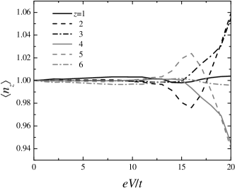
Let us first check if the assumption of linear potential is reasonable or not. Figure 2 plots the charge densities as a function of applied bias voltage for a heterostructure with . As can be seen, the charge densities are essentially unchanged up to (deviation from is smaller than 1%; it is about 6% even at high voltage ). Therefore, the assumption of a -linear potential is rather realistic.
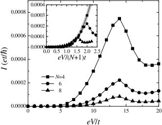
Next we discuss the current-voltage (-) characteristics of the Hubbard heterostructures. Numerical results are shown in Fig. 3. The thickness of the interaction region is changed as , and 8. For small voltages , current is exponentially small. The current grows rapidly above , and it continues up to , above which it begins to decrease. Such a behavior is similar to that of a conventional metal–band-insulator–metal junction with the gap amplitude and the distance from the middle of the gap to the top of the conduction band (or the bottom of the valence band) . Thus the -axis transport is expected to be due to the interband Zener tunneling as discussed in Ref. Oka03, , in particular in the low voltage region. In Ref. Oka03, , breakdown of one-dimensional Mott insulators by an applied voltage is investigated using a finite-size Hubbard ring. The applied voltage is introduced by a time-dependent vector potential.
This picture is further supported by replotting the current as a function of electric field . The result is shown in the inset of Fig. 3. As can be seen, the current at the low voltage region () falls onto the universal curve given by with fitting parameters as indicated by a light line. Similar results have been reported by Al-Hassanieh and co-workers who performed time-dependent density-matrix-renormalization group (DMRG) studies on one-dimensional heterostructures with a Mott-insulating region sandwiched by noninteracting leads.Al-Hassanieh07 This may indicate that the conventional band-insulator-like transport behavior is common for the Mott insulator in all dimensions. However, there has not been a direct observation confirming the Zener tunneling in correlated insulators. This is because the numerical methods used in the previous studies deal with the time evolution of the ground state under a time-dependent external field. So it is difficult to see the electron spectral function in the steady state. On the other hand, the present formalism directly deals with the steady state.
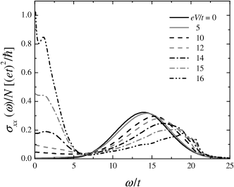
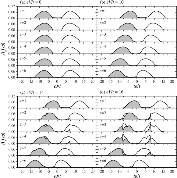
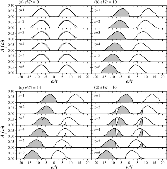
Figure 4 shows the layer-resolved spectral functions for Hubbard heterostructure with several choices of bias voltage. Other parameters are the same as in Figs. 2 and 3. Occupied regions, i.e., , are shaded. Figures 4 (a)– 4(c) confirm the naive interpretation based on the conventional band insulator; about of Mott gap is evident from (a); a chemical potential of lead () is located inside the upper Hubbard bands (b), and touches the top of the upper Hubbard band of the layer at at (c). Above (d), another tunneling process sets in from the top of the upper Hubbard band for layers to the unoccupied state of lead , resulting in a negative differential conductance. At low bias voltage , the deformation of spectral functions is very weak because the amount of electrons injected in the upper Hubbard band (and holes injected in the lower Hubbard band) is too small (see also the voltage dependent charge densities in Fig. 2). Therefore the magnitude of the gap controls the -axis transport which is less sensitive to the detail of the model. This confirms the Zener tunneling mechanism.
In addition to the “rigid” shift of the layer-dependent spectral functions, quasiparticle-like sharp features are visible in the spectral functions at in the high bias voltage region as seen in Figs. 4 (c) and 4 (d). In the equilibrium case, such quasiparticle features are observed only at the Fermi level. In the current nonequilibrium case, it is possible to have two “quasiparticle” peaks at as in the nonequilibrium quantum dot.Meir91 The existence of quasiparticles may indicate metallic transport properties, i.e., larger current densities. However, with the parameters used here, quasiparticle features appear at rather high voltage and the additional tunneling process sets in as discussed above. Therefore the current density is not enhanced. It would be very interesting to investigate the nonequilibrium behavior of correlated heterostructures with a smaller parameter (close to the critical value for the bulk Mott transition). If the “quasiparticle” structures appear before the chemical potential exceeds the upper edge of the spectral function at the rightmost layer, it would induce a larger current, resulting in highly nonlinear - characteristics. Such a study requires impurity solvers suitable for weaker interactions.
Layer-resolved spectral functions deformed by an applied bias voltage are essentially measurable by photoemission spectroscopy (PES) and scanning tunneling microscopy (STM). Yet, in light of the available spatial resolution, the latter seems plausible. Since, a current is already injected by an applied voltage, the insulating nature of the sample would not be a problem for STM. Although indirect, optical conductivity measurements might also be useful to investigate deformed spectral functions. Using Eq. (15), in-plane optical conductivity spectra are computed for Hubbard heterostructure with several choices of bias voltage as shown in Fig. 5. Other parameters are the same as in Figs. 2–4. At low bias voltage, the spectrum is dominated by an inter-Hubbard-band transition appearing at . With increasing bias voltage, the peak position of the inter-Hubbard-band transition shifts upwards because of the change in the potential profile in the interacting region. The weight of the inter-Hubbard-band transition is reduced and transferred to the low frequency region. The Drude-like low frequency structure is rather broad until sharp resonancelike structures become clear in the spectral functions. In the actual optical conductivity measurement, one needs a rather thick interacting region compared with the radius of the incident light. Otherwise, the huge Drude response from the noninteracting leads would hide the low frequency features coming from the interacting region.
Comparison with Falicov-Kimball model
In order to see the effect of the change in spectral functions, in particular the evolution of quasiparticle peaks, on the current-voltage characteristics, we have also applied the current DMFT method to the spinless Falicov-Kimball (FK) model. In this model, itinerant fermions described by interact with localized fermions via the on-site Coulomb interaction .Falicov69 It is known that, when , the FK model does not exhibit a quasiparticle feature unlike the Hubbard model.Si92 We take the local interaction as and the transfer intensity of fermions as so that the positions of the upper- and lower-Hubbard bands and the magnitude of Mott gap become similar to those of the Hubbard model with studied in the previous section.
The -fermion self-energy of the FK model has the same form as the electron self-energy of the Hubbard model given in Eq. (13) with and replaced with . For the computation, we fixed the mean density of fermions at each layer as for all applied bias voltage.
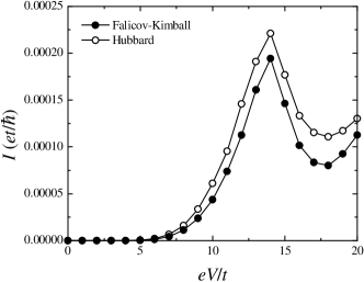
Numerical results for the layer-resolved spectral functions of itinerant fermions for FK-model heterostructure are shown in Fig. 6 with several choices of bias voltage indicated. As seen in Fig. 6 (a), the inter-Hubbard-band peak-to-peak distance and the gap amplitude of the FK heterostructure are almost identical to those of the Hubbard heterostructure. It is also evident that the spectral functions of the FK heterostructure are less sensitive to the bias voltage and do not show the resonance feature unlike the Hubbard heterostructure (see Fig. 4 for comparison). In the FK model, electric current is carried only by the itinerant fermions. Numerical results for the current-voltage characteristics of FK heterostructure are shown as filled circles in Fig. 7. For comparison, the current per spin as a function of bias voltage for Hubbard heterostructure with is also shown as open circles. At first sight, the similarity in the - characteristics is remarkable between the Hubbard and the FK heterostructures. This clearly demonstrates that the -axis transport properties of metal–Mott-insulator–metal heterostructures is dominated by the inter-Hubbard-band tunneling. Yet, about 10% (20%) enhancement of the current at can be seen in the Hubbard heterostructure despite a factor 2/3 smaller transfer intensity than in the FK heterostructure. This originates from the faster narrowing of the Mott gap by an applied bias voltage in the Hubbard heterostructures than in the FK heterostructures. To see this behavior semiquantitatively, let us define the gap amplitude by the width in which the spectral function becomes smaller than 0.001. Note that the spectral function is finite everywhere and, strictly speaking, there is no gap at finite temperature and bias voltage. By this definition, the gap amplitude at is estimated to be at layer in Hubbard heterostructure, and at layer in FK heterostructure, i.e., the former is about 40% smaller than the latter. Thus the effect of dynamical fluctuations in the Hubbard heterostructure is rather strong, overcoming the narrower bandwidth and enhancing the current amplitude.
IV Summary and Discussion
Summarizing, we have investigated the electronic properties of metal–Mott-insulator–metal heterostructures under an applied bias voltage between the metallic leads by employing the dynamical-mean-field theory combined with the Keldysh Green’s function technique. We have focused on the strong coupling region. In this case, the current-voltage characteristics of Hubbard heterostrucures were found to be quite similar to that of the conventional metal-semiconductor-metal heterostructures. Similar current-voltage characteristics are also obtained by using the Falicov-Kimball model in which itinerant fermions do not exhibit a quasiparticle feature.Si92 These findings indicate that the electron transport in correlated-insulator heterostructures is mainly dominated by inter-Hubbard-band tunneling. On the other hand, the electron spectral functions are strongly deformed by an applied voltage. Deformed spectral functions under a finite bias voltage are measurable by using (spatially resolved) photoemission spectroscopy and scanning tunneling microscopy. Such effects may also be examined by optical conductivity measurements.
Doped case
So far, we have considered the particle-hole symmetric situation before applying a bias voltage. Here we consider the hole-doped situation by increasing the potential at all layers by with the other parameters unchanged. As in the undoped case, we assume that the potential in the central region varies linearly as interpolating and . In a realistic situation, this assumption is not fully justified because an external electric field is screened by the redistribution of carriers and the potential drop occurs only near the interface regions. In order to describe such a screening effect, it is necessary to introduce a long-range Coulomb interaction and to determine the potential profile by solving the Poisson equation self-consistently. These effects are neglected in this study. Nevertheless, the qualitative behavior including the linear current-voltage characteristics and the change in quasiparticle features presented below is expected to be unchanged.
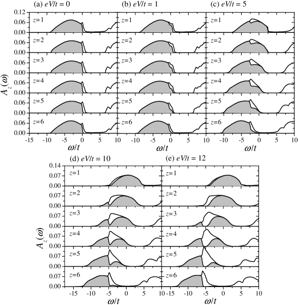
Numerical results for the layer-resolved spectral functions are shown in Fig. 8. At low bias voltage, the splitting of the resonance structure can be seen [Fig. 8 (b)]. This is similar to the nonequilibrium Kondo effect in the quantum dots.Meir91 With increasing , higher peaks are moved inside the Mott gap, and only the lower peaks remain visible. Because the electric current is carried by the quaiparticles in the metallic region, the change in the spectral function by a bias voltage may affect the current-voltage characteristics.
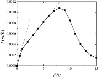
The current-voltage characteristic of the doped Hubbard heterostructure is shown in Fig. 9. Near-linear voltage dependence of current can be seen at low voltage with the change of slope at as indicated by dashed lines. This change is due to the disappearance of one of the two resonance peaks.
The frequency dependent electron occupation in the doped Hubbard heterostructure is changed more drastically. As shown in Fig. 8 (e), holes are injected into the lower Hubbard band more strongly than in the undoped case (see Fig. 4 for comparison). Thus the electron density becomes completely depressed in some frequency regions (see layers at ). These features may affect excitations, i.e., the optical conductivity, more strongly than in the undoped case.
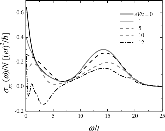
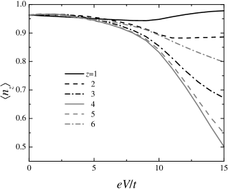
Numerical results for the in-plane optical conductivity of the doped Hubbard heterostructure are shown in Fig. 10 for several choices of bias voltage indicated. Contrary to the Mott-insulator heterostructure, an applied bias voltage destroys the low frequency Drude-like peak efficiently. An applied bias voltage also reduces the total weight correlated with the reduction of electron density inside the interacting region as shown in Fig. 11. The reduced electron density strongly depends on the layer, indicating the emergence of a “dipole” moment. Therefore, in a more realistic calculation, it will be necessary to include the long-ranged Coulomb interaction and determine the potential profile self-consistently.Okamoto04b We are currently working on including such effects under various situations. The two-peak structure in the spectral function seen in Fig. 8 (b) is hardly observable in the optical conductivity. This may be because the electron distribution functions have a similar structure to the spectral functions, effectively reducing the contribution from the interpeak transition. As can be seen from the shaded area, has a two-step structure. Further, the finite imaginary part of the self-energy broadens the structure in the optical conductivity even if it exists.
Another interesting observation is the emergence of the negative conductivity (see the result for in Fig. 10). The negative conductivity should be remedied by including the vertex correction. Yet, it implies the optical response of the correlated system becomes unusual in the nonequilibrium situation. This may be an interesting future problem.
Other work and future prospects
Nonequilibrium transport properties of one-dimensional metal–Mott-insulator-metal heterostructures have also been studied by Yonemitsu.Yonemitsu05 His main focus is on the field-effect carrier injection by an applied gate voltage, and he points out that the ambipolar current-voltage characteristics is a general feature of metal–Mott-insulator-metal heterostructures. In contrast to the behavior of conventional metal–band-insulator–metal heterostructures, ambipolar behavior is found to be insensitive to the difference in the work function between the Mott insulator and the metallic leads. On the other hand, in light of our results, Mott insulators and band insulators are expected to behave quite similarly. Thus the difference comes from the absence of long-range Coulomb interaction and the difference in the work function between the sample and leads in our case. Including these effects is certainly necessary for applying the current DMFT method to the more realistic system. Yet, there may appear further interesting phenomena in higher dimension; in this case, quasiparticle structure at the Fermi level emerges more easily than in the particle-hole symmetric case studied here.
Another work on one-dimensional heterostructures was performed by Oka and Nagaosa.Oka05 They applied the DMRG technique to study the charge density redistribution in the interface between noninteracting metal and correlated-metal in the presence of work function difference between the two. Even though they are dealing with one-dimensional models in which quantum effects are strongest, density profiles were found to be well reproduced by using the classical charge with the appropriate gap at an integer-filling region. This observation about the static properties is actually consistent with the previous studies on the higher-dimensional heterostructures. It has been shown that the static charge profile computed by DMFT is almost identical to the one by the mean-field approximation.Freericks01 ; Okamoto04b Based on this finding, they proposed an interesting “interface Mott transition” to explain the colossal electroresistance, i.e., the large switching of resistance by an applied bias voltage, observed experimentally.Bikalov03 ; Sawa04 Their assumption is that the filling-controlled Mott metal-insulator transition occurs by applying a bias voltage, and that the Mott transition is of the first order in higher-than-one dimensions. The Mott metal-insulator transition in the higher dimension is characterized by a collapse of the small energy scale which is roughly the quasiparticle bandwidth.Georges96 Therefore, in order to have a first order transition, the temperature must be smaller than this energy scale. On the other hand, applying a bias voltage has a similar effect to increasing the temperature. Therefore if the bias voltage required to accomplish the integer filling at some layer becomes larger than the small energy scale, the metal-insulator transition would become of the second order or just a crossover. A very interesting theoretical question is whether an interface Mott transition is really possible.
In this paper, we have focused only on a paramagnetic phase and “Mott” physics. However in general, correlated electron systems have a strong tendency toward magnetic ordering. A single-band Hubbard model is known to exhibit an antiferromagnetic ordering at half-filling. This ordering is affected by applying a magnetic field, changing the chemical potentials by a gate voltage, or injecting a current by applying a bias voltage. In any of these cases, the current-voltage characteristics are expected to be modified from the results obtained in this paper. Therefore including magnetic symmetry breaking is one of the interesting extensions of this work. It is also possible and desirable to consider magnetic leads instead of non-magnetic ones. This is of the direct relevance to the TMR effect.
Further, application of the present DMFT method to other models is highly desirable. This includes the double-exchange model (with electron-phonon coupling) for CMR manganites, and the multiorbital Hubbard model for general transition-metal oxides. For either model, fluctuation, ordering or melting of internal degrees of freedom would affect the transport properties of heterostructures. Controlling these degrees of freedom by external fields including a bias voltage and exploring the new phenomena that arise are important and urgent tasks.
Another possible extension is including spatial correlation beyond single-site DMFT. As the mathematical structure of the EOM method used in this paper is quite similar to that of so called correlator projection method,Onoda03 generalizing the current method to the multisite problem would not be so difficult.
Acknowledgements.
The author thanks E. Dagotto, K. A. Al-Hassanieh, R. S. Fishman, X.-G Zhang, A. H. Castro Neto, J. K. Freericks, J. E. Han, A. J. Millis, and I. Zutic for valuable discussions and R. S. Fishman for critical reading of the manuscript. This work was supported by the Division of Materials Sciences and Engineering, Office of Basic Energy Sciences, U.S. Department of Energy, under Contract No. DE-AC05-00OR22725 with Oak Ridge National Laboratory, managed and operated by UT-Battelle, LLC.References
- (1) M. Imada, A. Fujimori, and Y. Tokura, Rev. Mod. Phys. 70, 1039 (1998).
- (2) M. Kawasaki, K. Takahashi, T. Maeda, R. Tsuchiya, M. Shinohara, O. Ishiyama, T. Yonezawa, M. Yoshimoto, and H. Koinuma, Science 266, 1540 (1994).
- (3) C. H. Ahn, S. Gariglio, P. Paruch, T. Tybell, L. Antognazza, and J.-M. Triscone, Science 284, 1152 (1999).
- (4) M. Izumi, Y. Ogimoto, Y. Konishi, T. Manako, M. Kawasaki, and Y. Tokura, Mater. Sci. Eng., B 84, 53 (2001).
- (5) S. Gariglio, C.H. Ahn, D. Matthey, and J.-M. Triscone, Phys. Rev. Lett. 88, 067002 (2002).
- (6) A. Ohtomo, D. A. Muller, J. L. Grazul, and H. Y. Hwang, Nature (London) 419, 378 (2002).
- (7) P. E. Batson, Nature (London) 366, 727 (1993).
- (8) D. A. Muller, Y. Tzou, R. Raj, and J. Silcox, Nature (London) 366, 725 (1993).
- (9) N. D. Browning, M. M. Chisholm, and S. J. Pennycook, Nature (London) 366, 143 (1993).
- (10) I. Bozovic, G. Logvenov, M. A. J. Verhoeven, P. Caputo, E. Goldobin, and M. R. Beasley, Nature (London) 422, 873 (2003).
- (11) I. Bozovic, G. Logvenov, M. A. J. Verhoeven, P. Caputo, E. Goldobin, and M. R. Beasley, Phys. Rev. Lett. 93, 157002 (2004).
- (12) J. Z. Sun, W. J. Gallagher, P. R. Duncombe, L. Krusin-Elbaum, R. A. Altman, A. Gupta, Yu Lu, G. Q. Gong, and G. Xiao, Appl. Phys. Lett. 69, 3266 (1996).
- (13) M. Bowen, M. Bibes, A. Barthélémy, J.-P. Contour, A. Anane, Y. Lemaître, and A. Fert, Appl. Phys. Lett. 82, 233 (2003).
- (14) J. K. Freericks, Phys. Rev. B 70, 195342 (2004).
- (15) S. Okamoto and A. J. Millis, Nature (London) 428, 630 (2004); Phys. Rev. B 70, 075101 (2004); 72, 235108 (2005); S. Okamoto, A. J. Millis, and N. A. Spaldin, Phys. Rev. Lett. 97, 056802 (2006).
- (16) S. Okamoto and A. J. Millis, Phys. Rev. B 70, 241104(R) (2004).
- (17) T. Oka and N. Nagaosa, Phys. Rev. Lett. 95, 266403 (2005).
- (18) W.-C. Lee and A. H. MacDonald, Phys. Rev. B 74, 075106 (2006).
- (19) S. S. Kancharla and E. Dagotto, Phys. Rev. B 74, 195427 (2006).
- (20) L. Esaki, Phys. Rev. 109, 603 (1958).
- (21) B. D. Josephson, Phys. Lett. 1, 251 (1962).
- (22) I. Giaever, Rev. Mod. Phys. 46, 245 (1974).
- (23) A. Georges, B. G. Kotliar, W. Krauth, and M. J. Rozenberg, Rev. Mod. Phys. 68, 13 (1996).
- (24) L. V. Keldysh, J. Exp. Theor. Phys. 47, 1515 (1964) [Sov. Phys. JETP 20, 1018 (1965)].
- (25) C. Caroli, R. Combescot, P. Nozieres, and D. Saint-James, J. Phys. C 4, 916 (1971).
- (26) S. Datta, in Electronic Transport in Mesoscopic Systems (Cambridge University Press, Cambridge, England, 1995).
- (27) M. Potthoff and W. Nolting, Phys. Rev. B 59, 2549; 60, 7834 (1999).
- (28) J. K. Freericks, B. K. Nikolić, and P. Miller, Phys. Rev. B 64, 054511 (2001).
- (29) P. Schmidt and H. Monien, arXiv:cond-mat/0202046.
- (30) J. K. Freericks, V. M. Turkowski, and V. Zlatić, Phys. Rev. Lett. 97, 266408 (2006).
- (31) J. A. Appelbaum and D. R. Penn, Phys. Rev. 188, 874 (1969).
- (32) C. Lacroix, J. Phys. F 11, 2389 (1981).
- (33) Y. Meir, N. S. Wingreen, and P. A. Lee, Phys. Rev. Lett. 66, 3048 (1991).
- (34) C. Gros, Phys. Rev. B 50, 7295 (1994).
- (35) H. O. Jeschke and G. Kotliar, Phys. Rev. B 71, 085103 (2005).
- (36) J.-X. Zhu, R. C. Albers, and J. M. Wills, Mod. Phys. Lett. B 20, 1629 (2006).
- (37) H. Kajueter and G. Kotliar, Phys. Rev. Lett. 77, 131 (1996).
- (38) T. Fujii and K. Ueda, Phys. Rev. B 68, 155310 (2003).
- (39) S. Hershfield, J. H. Davies, and J. W. Wilkins, Phys. Rev. Lett. 67, 3720 (1991).
- (40) T. Pruschke, D. L. Cox, and M. Jarrell, Phys. Rev. B 47, 3553 (1993).
- (41) A. N. Rubtsov, V. V. Savkin, and A. I. Lichtenstein, Phys. Rev. B 72, 035122 (2005).
- (42) P. Werner, A. Comanac, L. de’ Medici, M. Troyer, and A. J. Millis, Phys. Rev. Lett. 97, 076405 (2006).
- (43) See, for example, E. M. Lifshits and L. P. Pitaevskii, Physical Kinetics (Pergamon, Oxford, 1981), Chap. 10.
- (44) T. Oka, R. Arita, and H. Aoki, Phys. Rev. Lett. 91, 066406 (2003).
- (45) K. A. Al-Hassanieh, A. E. Feiguin, F. Heidrich Meisner, I. Gonzalez, M. J. Rozenberg, and E. Dagotto (unpublished).
- (46) L. M. Falicov and J. C. Kimball, Phys. Rev. Lett. 22, 997 (1969).
- (47) Q. Si, G. Kotliar, and A. Georges, Phys. Rev. B 46, 1261 (1992).
- (48) K. Yonemitsu, J. Phys. Soc. Jpn. 74, 2671 (2005).
- (49) A. Baikalov, Y. Q. Wang, B. Shen, B. Lorenz, S. Tsui, Y. Y. Sun, Y. Y. Xue, and C. W. Chu, Appl. Phys. Lett. 83, 957 (2003).
- (50) A. Sawa, T. Fujii, M. Kawasaki, and Y. Tokura, Appl. Phys. Lett. 85, 4073 (2004).
- (51) S. Onoda and M. Imada, Phys. Rev. B 67, 161102(R) (2003).