Present address: ] Department of Physics and Astronomy, University of British Columbia, Vancouver, British Columbia V6T-1Z1, Canada
Hard x-ray photoemission study of LaAlO3/LaVO3 multilayers
Abstract
We have studied the electronic structure of multilayers composed of a band insulator LaAlO3 (LAO) and a Mott insulator LaVO3 (LVO) by means of hard x-ray photoemission spectroscopy, which has a probing depth as large as . The Mott-Hubbard gap of LVO remained open at the interface, indicating that the interface is insulating unlike the LaTiO3/SrTiO3 multilayers. We found that the valence of V in LVO were partially converted from V3+ to V4+ only at the interface on the top side of the LVO layer and that the amount of V4+ increased with LVO layer thickness. We suggest that the electronic reconstruction to eliminate the polarity catastrophe inherent in the polar heterostructure is the origin of the highly asymmetric valence change at the LVO/LAO interfaces.
pacs:
71.28.+d, 73.20.-r, 79.60.Dp, 71.30.+hI Introduction
The interfaces of hetero-junctions composed of transition-metal oxides have recently attracted great interest. For example, it has been suggested that the interface between a band insulator SrTiO3 (STO) and a Mott insulator LaTiO3 (LTO) shows metallic conductivity. HwangTi ; shibuyaLTOSTO ; okamotoLTOSTO Recently, Takizawa et al. takizawaLTOSTO measured photoemission spectra of this interface and observed a clear Fermi cut-off, indicating that an electronic reconstruction indeed occurs at this interface. In the case of STO/LTO, electrons penetrate from the layers of the Mott insulator to the layers of the band insulator, resulting in the intermediate band filling and hence the metallic conductivity of the interfaces. It is therefore interesting to investigate how electrons behave if we confine electrons in the layers of the Mott insulator. In this paper, we investigate the electronic structure of multilayers consisting of a band insulator LaAlO3 (LAO) and a Mott insulator LaVO3 (LVO). LAO is a band insulator with a large band gap of about 5.6 eV. LVO is a Mott-Hubbard insulator with a band gap of about 1.0 eV. opt1 This material shows G-type orbital ordering and C-type spin ordering below the transition temperature K. LVO2 From the previous results of photoemission and inverse photoemission spectroscopy, it was revealed that in the valence band there are O bands at eV and V bands (lower Hubbard bands; LHB) at eV and that above there are upper Hubbard bands (UHB) of V origin separated by a band gap of about 1 eV from the LHB. Maiti Since the bottom of the conduction band of LAO has predominantly La character and its energy position is well above that of the LHB of LVO, LAO the V electrons are expected to be confined within the LVO layers as a “quantum well” and not to penetrate into the LAO layers, making this interface insulating unlike the LTO/STO case. HwangTi ; shibuyaLTOSTO ; okamotoLTOSTO ; takizawaLTOSTO Recently, Hotta et al. Hotta investigated the electronic structure of 1-5 unit cell thick layers of LVO embedded in LAO by means of soft x-ray (SX) photoemission spectroscopy. They found that the V core-level spectra had both V3+ and V4+ components and that the V4+ was localized in the topmost layer. However, due to the surface sensitivity of SX photoemission, the information about deeply buried interfaces in the multilayers is still lacking. Also, they used an unmonochromatized x-ray source, whose energy resolution was not sufficient for detailed studies of the valence band. In the present work, we have investigated the electronic structure of the LAO/LVO interfaces by means of hard x-ray (HX) photoemission spectroscopy ( eV) at SPring-8 BL29XU. HX photoemission spectroscopy is a bulk-sensitive experimental technique compared with ultraviolet and SX photoemission spectroscopy, and is very powerful for investigating buried interfaces in multilayers. From the valence-band spectra, we found that a Mott-Hubbard gap of LVO remained open at the interface, indicating the insulating nature of this interface. From the V and core-level spectra, the valence of V in LVO was found to be partially converted from V3+ to V4+ at the interface, confirming the previous study. Hotta Furthermore, the amount of V3+ was found to increase with LVO layer thickness. We attribute this valence change to the electronic reconstruction due to polarity of the layers.
II Experiment
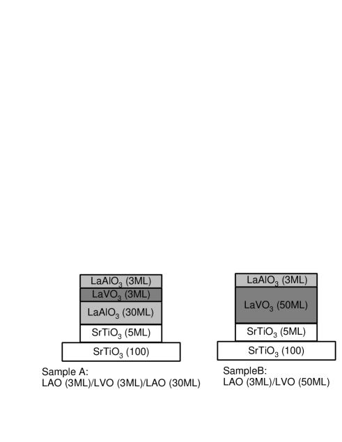
The LAO/LVO multilayer thin films were fabricated on TiO2-terminated STO substrates Kawasaki using the pulsed laser deposition (PLD) technique. An infrared heating system was used for heating the substrates. The films were grown on the substrates at an oxygen pressure of Torr using a KrF excimer laser ( nm) operating at 4 Hz. The laser fluency to ablate LaVO4 polycrystalline and LAO single crystal targets was J/cm2. The film growth was monitored using real-time reflection high-energy electron diffraction (RHEED). Schematic views of the fabricated thin films are shown in Fig. 1. Sample A consisted of 3ML LVO capped with 3ML LAO. Below the 3ML LVO, 30ML LAO was grown, making LVO sandwiched by LAO. Sample B consisted of 50ML LVO capped with 3ML LAO. Sample C was 50ML LVO without LAO capping layers. Details of the fabrication and characterization of the films were described elsewhere. HottaLVO The characterization of the electronic structure of uncapped LaVO3 thin films by x-ray photoemission spectroscopy will be described elsewhere. WadatiuncapLVO HX photoemission experiments were performed at an undulator beamline, BL29XU, of SPring-8. The experimental details are described in Refs. TamasakuHardX, ; IshikawaHardX, ; HardX, . The total energy resolution was set to about 180 meV. All the spectra were measured at room temperature. The Fermi level () position was determined by measuring gold spectra.
III Results and discussion
Figure 2 shows the valence-band photoemission spectra of the LAO/LVO multilayer samples. Figure 2 (a) shows the entire valence-band region. Compared with the previous photoemission results, Maiti structures from 9 to 3 eV are assigned to the O dominant bands, and emission from 3 eV to to the V bands. The energy positions of the O bands were almost the same in these three samples, indicating that the band bending effect at the interface of LAO and LVO was negligible. Figure 2 (b) shows an enlarged plot of the spectra in the V -band region. A Mott-Hubbard gap of LVO remained open at the interface between LAO and LVO, indicating that this interface is insulating unlike the STO/LTO interfaces. HwangTi ; shibuyaLTOSTO ; okamotoLTOSTO ; takizawaLTOSTO The line shapes of the V bands were almost the same in these three samples, except for the energy shift in sample A. We estimated the value of the band gap from the linear extrapolation of the rising part of the peak as shown in Fig. 2 (b). The gap size of sample B was almost the same ( meV) as that of sample C, while that of sample A was much larger ( meV) due to the energy shift of the V bands. The origin of the enhanced energy gap is unclear at present, but an increase of the on-site Coulomb repulsion in the thin LVO layers compared to the thick LVO layers or bulk LVO due to a decrease of dielectric screening may explain the experimental observation.
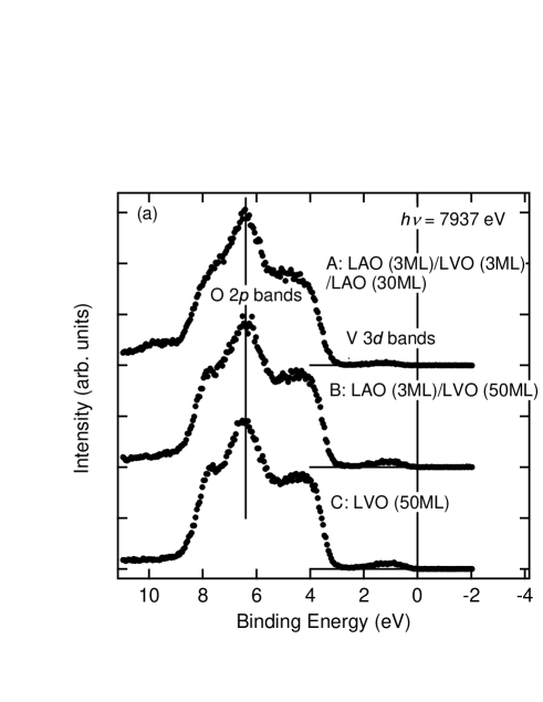
Figure 3 shows the V core-level photoemission spectra of the LAO/LVO multilayer samples. The V spectra had a main peak at 5467 eV and a satellite structure at 5478 eV. The main peaks were not simple symmetric peaks but exhibited complex line shapes. We therefore consider that the main peaks consisted of V3+ and V4+ components. In sample C, there is a considerable amount of V4+ probably due to the oxidation of the surface of the uncapped LVO. A satellite structure has also been observed in the V spectrum of V2O3 kamakura and interpreted as a charge transfer (CT) satellites arising from the final state, where denotes a hole in the O band. Screening-derived peaks at the lower-binding-energy side of V , which have been observed in the metallic phase of V2-xCrxO3, kamakura ; taguchi were not observed in the present samples, again indicating the insulating nature of these interfaces.
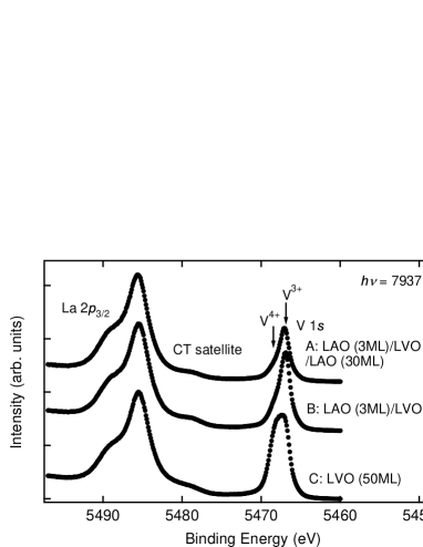
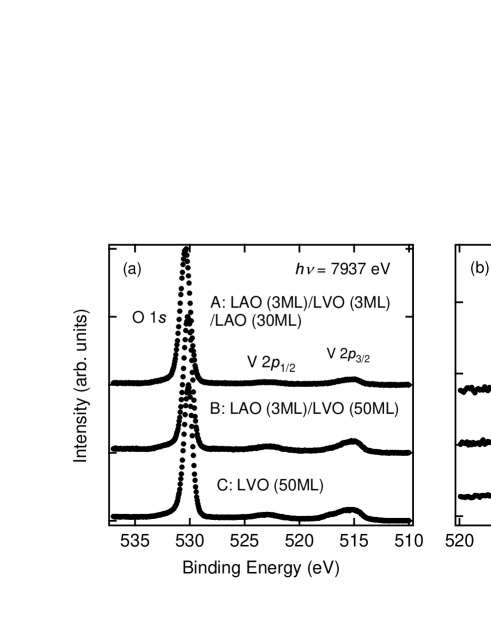
Figure 4 shows the O and V core-level photoemission spectra of the LAO/LVO multilayer samples. The O spectra consisted of single peaks without surface contamination signal on the higher-binding-energy side, indicating the bulk sensitivity of HX photoemission spectroscopy. The energy position of the O peak of sample A, whose LVO layer thickness was only 3 ML, was different from those of the rest because LAO and LVO have different energy positions of the O core levels. Figure 4 (b) shows an enlarged plot of the V spectra. Here again, the V photoemission spectra showed complex line shapes consisting of V3+ and V4+ components, and no screening-derived peaks on the lower-binding-energy side of V were observed. The line shapes of the V spectra were very similar for samples A and B. The amount of V4+ was larger in sample C, consistent with the case of V and again shows the effect of the oxidation of the uncapped LVO.
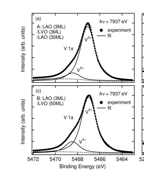
We have fitted the core-level spectra of samples A and B to a Gaussian convoluted with a Lorentzian to estimate the amount of V3+, V4+ and V5+ at the interface following the procedure of Ref. Hotta, . Figure 5 shows the fitting results of the V and V core-level spectra. Here, the spectra were decomposed into the V3+ and V4+ components, and the V5+ component was not necessary. The full width at half maximum (FWHM) of the Lorentzian has been fixed to 1.01 eV for V and to 0.24 eV for V according to Ref. width, . The FWHM of the Gaussian has been chosen 0.90 eV for V and 1.87 eV for V , reflecting the larger multiplet splitting for V than for V . In Fig. 6, we summarize the ratio of the V3+ component thus estimated, together with the results of the emission angle () dependence of the V core-level SX photoemission spectra measured using a laboratory SX source. Hotta
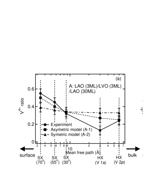
In order to interpret those results qualitatively, first we have to know the probing depth of photoemission spectroscopy under various measurement conditions. From the kinetic energies of photoelectrons, the mean free paths of the respective measurements are obtained as described in Ref. Tanuma, . foot When we measure V spectra with the Mg K line ( eV), the kinetic energy of photoelectrons is about 700 eV, and the mean free path is estimated to be about 10 Å. Likewise, we also estimate the mean free path in the HX case. The values are summarized in Table 1. In the SX case, these values are Å. One can obtain the most surface-sensitive spectra under the condition of SX with [denoted by SX(70o)] and the most bulk-sensitive spectra for HX measurements of the V core level [denoted by HX(V )]. From Fig. 6 and Table 1, one observes a larger amount of V4+ components under more surface-sensitive conditions. These results demonstrate that the valence of V in LVO is partially converted from V3+ to V4+ at the interface.
| SX | SX | SX | HX | HX |
| (70∘) | (55∘) | (30∘) | (V ) | (V ) |
| 3.4 | 5.7 | 8.7 | 30 | 60 |
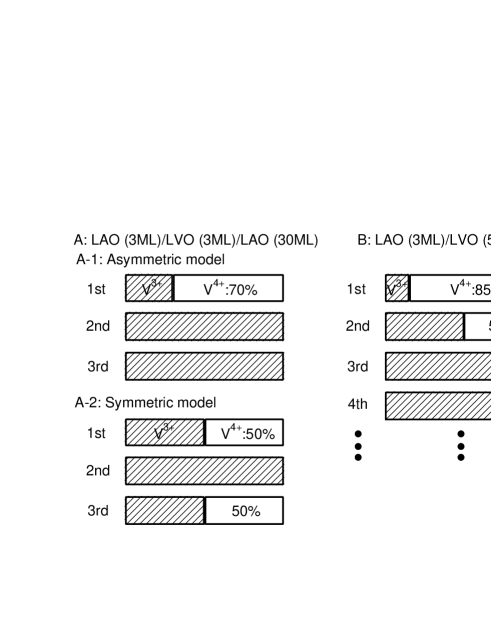
In order to reproduce the present experimental result and the result reported in Ref. Hotta, (shown in Fig. 6), we propose a model of the V valence distribution at the interface as shown in Fig. 7. For sample A, we consider two models, that is, an asymmetric model and a symmetric model. In the asymmetric model (A-1), no symmetry is assumed between the first and the third layers. As shown in Fig. 6, the best fit result was obtained for the valence distribution that 70 % of the first layer is V4+ and there are no V4+ in the second and third layers, assuming the above-mentioned mean free paths in Table 1 and exponential decrease of the number of photoelectrons. In the symmetric model (A-2), it is assumed that the electronic structures are symmetric between the first and the third layers. The best fit was obtained when 50 % of the first and third layers are V4+. In sample B, a model (B) where 85 % of the first layer and 50 % of the second layer are V4+ best reproduced the experimental result. As shown in Fig. 6, for the 3ML case, the model (A-2) did not reproduce the experimental results well compared to (A-1), which demonstrates that the valence distribution of V was highly asymmetric at these interfaces.
The origin of this highly asymmetric valence change from V3+ to V4+ at the interfaces can be interpreted in two ways. One possible scenario is a simple chemical effect during the fabrication process of the PLD technique. The topmost LVO layer spends a longer time before the next deposition of LAO than the rest LVO layers, and therefore, oxidation process may easily proceed at the topmost layer. In this scenario, if we make samples under different experimental conditions, especially under different oxygen pressures, the amount of V4+ at the interface may change greatly. In the other scenario, we consider that the polarity of the LAO/LVO multilayers plays an essential role. In the present samples, both the LAO and LVO layers are polar, and do not consist of charge neutral layers, that is, they consist of alternating stack of LaO+ and AlO or VO layers. As recently discussed by Nakagawa et al., nakagawa electronic reconstruction occurs during the fabrication of the polar layers in order to prevent the divergence of Madelung potential, i.e., so-called polar catastrophe. catas We consider that the electronic reconstruction occurs in the present samples, and that the valence change of V at the interface is a result of this reconstruction. This effect explains 0.5 ML of V4+, but we cannot explain the total amount of V4+ exceeding 0.5 ML, and we must also consider some chemical effects that V atoms are relatively easily oxidized at the topmost layer. Similar studies on samples with different termination layers will be necessary to test this scenario. Recently, Huijben et al. huijben studied STO/LAO multilayers and found a critical thickness of LAO and STO, below which a decrease of the interface conductivity and carrier density occurs. Therefore, changing the numbers of LAO capping layers may also change the valence of V at the interface. Further systematic studies, including other systems like LTO/STO HwangTi ; shibuyaLTOSTO ; okamotoLTOSTO ; takizawaLTOSTO and LAO/STO nakagawa ; huijben ; Hwang2 , will reveal the origin of the valence change at the interface.
IV conclusion
We have investigated the electronic structure of the multilayers composed of a band insulator LaAlO3 and a Mott insulator LaVO3 (LVO) by means of HX photoemission spectroscopy. The Mott-Hubbard gap of LVO remained open at the interface, indicating that the interface is insulating and the delocalization of electrons does not occur unlike the LaTiO3/SrTiO3 multilayers. From the V and core-level photoemission intensities, we found that the valence of V in LVO was partially converted from V3+ to V4+ at the interface only on the top side of the LVO layer and that the amount of V4+ increased with LVO layer thickness. We constructed a model for the V valence redistribution in order to explain the experimental result and found that the V4+ is preferentially distributed on the top of the LVO layers. We suggest that the electronic reconstruction to eliminate polar catastrophe may be the origin of the highly asymmetric valence change at the interfaces.
V acknowledgments
The HX photoemission experiments reported here have benefited tremendously from the efforts of Dr. D. Miwa of the coherent x-ray optics laboratory RIKEN/SPring-8, Japan and we dedicate this work to him. This work was supported by a Grant-in-Aid for Scientific Research (A16204024) from the Japan Society for the Promotion of Science (JSPS) and a Grant-in-Aid for Scientific Research in Priority Areas “Invention of Anomalous Quantum Materials” from the Ministry of Education, Culture, Sports, Science and Technology. H. W. acknowledges financial support from JSPS. Y. H. acknowledges support from QPEC, Graduate School of Engineering, University of Tokyo.
References
- (1) A. Ohtomo, D. A. Muller, J. L. Grazul, and H. Y. Hwang, Nature 419, 378 (2002).
- (2) K. Shibuya, T. Ohnishi, M. Kawasaki, H. Koinuma, and M. Lippmaa, Jpn. J. Appl. Phys. 43, L1178 (2004).
- (3) S. Okamoto and A. J. Millis, Nature 428, 630 (2004).
- (4) M. Takizawa, H. Wadati, K. Tanaka, M. Hashimoto, T. Yoshida, A. Fujimori, A. Chikamatsu, H. Kumigashira, M. Oshima, K. Shibuya, T. Mihara, T. Ohnishi, M. Lippmaa, M. Kawasaki, H. Koinuma, S. Okamoto, and A. J. Millis, Phys. Rev. Lett. 97, 057601 (2006).
- (5) T. Arima, Y. Tokura, and J. B. Torrance, Phys. Rev. B 48, 17006 (1993).
- (6) S. Miyasaka, Y. Okimoto, M. Iwama, and Y. Tokura, Phys. Rev. B 68, 100406(R) (2003).
- (7) K. Maiti and D. D. Sarma, Phys. Rev. B 61, 2525 (2000).
- (8) S.-G. Lim, S. Kriventsov, T. N. Jackson, J. H. Haeni, D. G. Schlom, A. M. Balbashov, R. Uecker, P. Reiche, J. L. Freeouf, and G. Lucovsky, J. Appl. Phys. 91, 4500 (2002).
- (9) Y. Hotta, H. Wadati, A. Fujimori, T. Susaki, and H. Y. Hwang, Appl. Phys. Lett. 89, 251916 (2006).
- (10) M. Kawasaki, K. Takahashi, T. Maeda, R. Tsuchiya, M. Shinohara, O. Ishihara, T. Yonezawa, M. Yoshimoto, and H. Koinuma, Science 266, 1540 (1994).
- (11) Y. Hotta, Y. Mukunoki, T. Susaki, H. Y. Hwang, L. Fitting, and D. A. Muller, Appl. Phys. Lett. 89, 031918 (2006).
- (12) H. Wadati, Y. Hotta, M. Takizawa, A. Fujimori, T. Susaki, and H. Y. Hwang (unpublished).
- (13) K. Tamasaku, Y. Tanaka, M. Yabashi, H. Yamazaki, N. Kawamura, M. Suzuki, and T. Ishikawa, Nucl. Instrum. Methods A 467/468, 686 (2001).
- (14) T. Ishikawa, K. Tamasaku, and M. Yabashi, Nucl. Instrum. Methods A 547, 42 (2005).
- (15) Y. Takata, M. Yabashi, K. Tamasaku, Y. Nishino, D. Miwa, T. Ishikawa, E. Ikenaga, K. Horiba, S. Shin, M. Arita, K. Shimada, H. Namatame, M. Taniguchi, H. Nohira, T. Hattori, S. Sodergren, B. Wannberg, and K. Kobayashi, Nucl. Instrum. Methods A 547, 50 (2005).
- (16) N. Kamakura, M. Taguchi, A. Chainani, Y. Takata, K. Horiba, K. Yamamoto, K. Tamasaku, Y. Nishino, D. Miwa, E. Ikenaga, M. Awaji, A. Takeuchi, H. Ohashi, Y. Senba, H. Namatame, M. Taniguchi, T. Ishikawa, K. Kobayashi, and S. Shin, Europhys. Lett. 68, 557 (2004).
- (17) M. Taguchi, A. Chainani, N. Kamakura, K. Horiba, Y. Takata, M. Yabashi, K. Tamasaku, Y. Nishino, D. Miwa, T. Ishikawa, S. Shin, E. Ikenaga, T. Yokoya, K. Kobayashi, T. Mochiku, K. Hirata, and K. Motoya, Phys. Rev. B 71, 155102 (2005).
- (18) M. O. Krause and J. H. Oliver, J. Phys. Chem. Ref. Data 8, 329 (1979).
- (19) S. Tanuma, C. J. Powell, and D. R. Penn, Surf. Sci. 192, L849 (1987).
- (20) The mean free paths in HX photoemission were recently determined experimentally as described in Refs. panac2004, ; panac, .
- (21) C. Dallera, L. Duo, L. Braicovich, G. Panaccione, G. Paolicelli, B. Cowie, and J. Zegenhagen, Appl. Phys. Lett. 85, 4532 (2004).
- (22) M. Sacchi, F. Offi, P. Torelli, A. Fondacaro, C. Spezzani, M. Cautero, G. Cautero, S. Huotari, M. Grioni, R. Delaunay, M. Fabrizioli, G. Vanko, G. Monaco, G. Paolicelli, G. Stefani, and G. Panaccione, Phys. Rev. B 71, 155117 (2005).
- (23) N. Nakagawa, H. Y. Hwang, and D. A. Muller, Nature Materials 5, 204 (2006).
- (24) W. A. Harrison, E. A. Kraut, J. R. Waldrop, and R. W. Grant, Phys. Rev. B 18, 4402 (1978).
- (25) M. Huijben, G. Rijnders, D. H. A. Blank, S. Bals, S. V. Aert, J. Verbeeck, G. V. Tendeloo, A. Brinkman, and H. Hilgenkamp, Nature Materials 5, 556 (2006).
- (26) A. Ohtomo and H. Y. Hwang, Nature 427, 423 (2004).