Mach–Zehnder-like interferometry with graphene nanoribbon networks
Abstract
We study theoretically electron interference in a Mach–Zehnder-like geometry formed by four zigzag graphene nanoribbons (ZGNRs) arranged in parallel pairs, one on top of the other, such that they form intersection angles of 60∘. Depending on the interribbon separation, each intersection can be tuned to act either as an electron beam splitter or as a mirror, enabling tuneable circuitry with interfering pathways. Based on the mean-field Hubbard model and Green’s function techniques, we evaluate the electron transport properties of such 8-terminal devices and identify pairs of terminals that are subject to self-interference. We further show that the scattering matrix formalism in the approximation of independent scattering at the four individual junctions provides accurate results as compared with the Green’s function description, allowing for a simple interpretation of the interference process between two dominant pathways. This enables us to characterize the device sensitivity to phase shifts from an external magnetic flux according to the Aharonov–Bohm effect as well as from small geometric variations in the two path lengths. The proposed devices could find applications as magnetic field sensors and as detectors of phase shifts induced by local scatterers on the different segments, such as adsorbates, impurities or defects. The setup could also be used to create and study quantum entanglement.
Keywords: Graphene nanoribbons, quantum transport, electron quantum optics, interferometry, spintronics, mean-field Hubbard model, Green’s functions, scattering matrix formalism \ioptwocol
1 Introduction
Over the past decade the field of electron quantum optics, where electrons play the role of photons in quantum-optics like experiments, has witnessed strong theoretical and experimental advances. For instance, several electronic analogues of optical setups have been implemented, such as the Mach–Zehnder [1, 2] and Fabry–Pérot [3, 4, 5] interferometers, as well as the Hanbury Brown–Twiss [6, 7, 8, 9] geometry, enabling studies of fermion antibunching and the two-particle Aharonov–Bohm [10] effect.
When it comes to electronic devices, graphene is an advantageous material showing a high degree of quantum coherence even at moderately high temperatures [11]. The similarities between electrons travelling ballistically in graphene constrictions and photons propagating in waveguides have placed the focus on this material for electron quantum optics applications. For instance, the electron wave nature has manifested in refraction effects in - junctions, e.g., when transmitted across a boundary separating regions of different doping levels [12, 13].
In particular, within the group of graphene derivatives and nanostructures, graphene nanoribbons (GNRs) offer attractive characteristics for electron quantum optics. First, the confinement of electrons to one dimension (1D) provides a versatile, width-dependent electronic structure which can include the appearance of a band gap and spin-polarized edge-states as, e.g., in the case of GNRs of zigzag edge topology (ZGNRs) [14, 15]. Secondly, it has been experimentally demonstrated that GNRs possess long coherence lengths, that can reach values of the order of nm [16, 17, 18]. Furthermore, ballistic transport in ZGNRs can be rather insensitive to edge defects because the current flows maximally through the center of the ribbon as a consequence of the dominating Dirac-like physics [19].
With respect to their experimental realization and feasibility, the emergence of bottom-up fabrication techniques has resulted in the fabrication of long, defect-free samples of GNRs via on-surface synthesis [20, 21, 22]. This approach has also opened new possibilities to design -magnetism in carbon nanostructures and to address localized, unpaired electron spins [23]. Additionally, GNRs can also be picked up and manipulated with scanning tunneling probes [24, 25, 26], suggesting the possibility of building two-dimensional multi-terminal GNR-based electronic circuits [27, 28, 29, 30, 31].
One of the most elementary building blocks necessary to perform electron quantum optics experiments is the electron beam splitter, the electronic analog of a beam splitter for light, which coherently splits an incoming particle into a superposition of two states propagating in different output arms of the device. Remarkably, it has been theoretically discovered that one GNR placed on top of another with an intersection angle close to enhances the electron transfer process between the ribbons, an effect related to the fact that the orientation of the honeycomb lattices of the bottom and top ribbons are aligned [32, 33, 34]. In fact, valence- or conduction-band electrons injected in such a four-terminal device are scattered into only two of the four possible outgoing directions without reflection. Depending on the width of the GNR, interlayer separation, and energy of the traversing electrons, the branching ratio can be varied, resulting in different behaviours such as mirrors, beam splitters (half-transparent mirrors), and energy filters [34]. Furthermore, the magnetic instabilities that appear due to the localization of the edge states in ZGNRs near the Fermi level [35, 14, 36] make junctions of ZGNRs even more interesting since they can spin-polarize the transmitted electrons [37].
With these fundamental components one can consider building a GNR-based Mach–Zehnder-like interferometer, which can be used for a variety of tasks from sensing of magnetic fluxes or local electric fields to measuring indistinguishability [9], statistics [38], and coherence length [39] of the charge carriers or generating entanglement between them [40, 41, 42]. Other two-path setups have been demonstrated to act as a manipulable flying qubit architecture [43] using the Aharonov–Bohm (AB) effect [44]. In graphene, the AB effect has been studied in ring-shaped nanostructures both theoretically [45, 46, 47, 48] and experimentally [49], and more recently also considered in bipolar hybrid monolayer-bilayer junctions [50]. It has also been observed in a graphene quantum-Hall system for spin- and valley-polarized edge states [51]. However, these nanostructures are in general difficult to produce. Moreover, when it comes to electron interference, clean systems and long phase-coherence length are required. Therefore, ZGNRs should provide an outstanding platform for electron quantum optics.
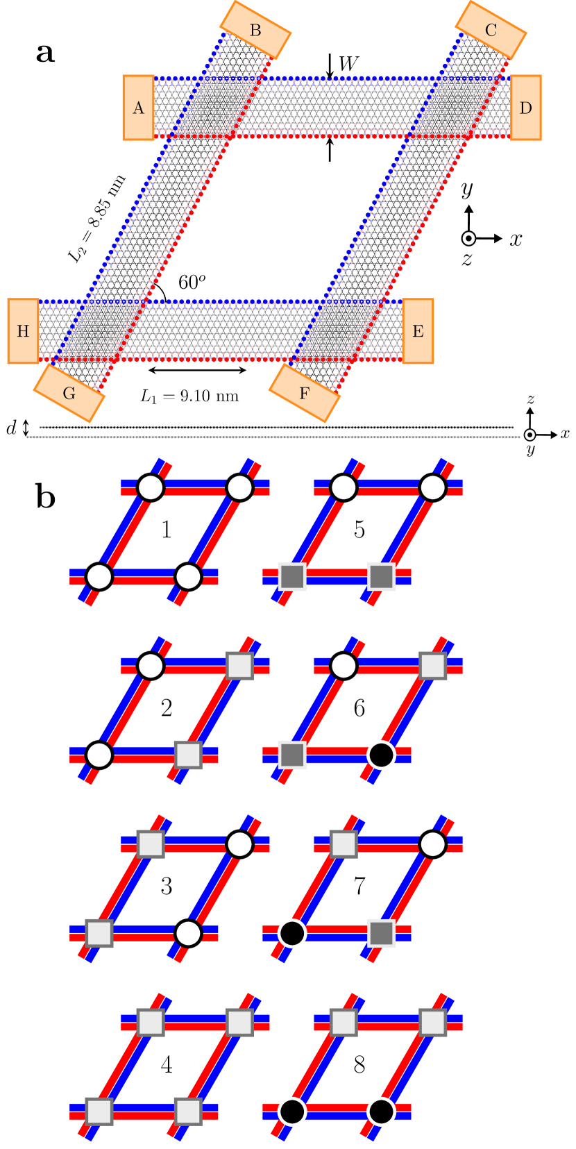
Here we propose a setup to study these phenomena which seem not too far away with the current experimental techniques. Our interferometer, shown in figure 1(a), is formed by four crossed ZGNRs in a pairwise arrangement forming a parallelogram where the intersecting angle between the ribbons is . The ZGNR width is here selected to be of 10 carbon atoms (); this choice is not particularly critical as qualitatively similar transport behavior is expected for other ribbon widths [34]. We show that in the single-channel energy window near the Fermi level, electrons are transmitted essentially without reflection at each intersection. This allows to describe the self-interference process by considering each junction as if they were independent scatterers for the incoming electrons. Given the exclusive transmission into only two out of the four terminals in each beam splitter, the AB effect in the multiterminal setup does not suffer from complicated multi-path interferences that would lead to the loss of quantum information carried by coherent electrons reaching the other reservoirs. This enables us to characterize the interferometer as a detector of phase shifts, e.g., induced by a transverse magnetic field, electric fields or any geometrical distortion or defect that changes the relative phase between the two available paths that will interfere.
2 Methods
2.1 Model Hamiltonian
The system, shown in figure 1(a), is divided into the device (scattering) region that contains the enclosed area by the crossing ribbons, and the eight semi-infinite ZGNRs (periodic electrodes), represented as orange rectangles. The total Hamiltonian is correspondingly split into the different parts , where is the device Hamiltonian, the -electrode Hamiltonian, and the coupling between these two subsystems.
The effective Hamiltonian for the -electrons, responsible for spin-polarization and transport phenomena, can be described in terms of the mean-field Hubbard (MFH) model with a single orbital per site [23, 52], i.e.,
| (1) |
where () creates (annihilates) an electron on site with spin , and is the number operator. The Coulomb interaction is parametrized via the onsite repulsion , which in the following is fixed to eV. The qualitative picture is not altered by its precise magnitude, only the quantitative results (like the size of the induced band gap). Following Ref. [34], the matrix element between orbitals and is described by Slater–Koster two-centre - and -type integrals between two atomic orbitals [53] as used previously for twisted bilayer graphene [54] and crossed GNRs [34, 37]. We further fix the on-site energies equal to the Fermi energy . Given that ZGNRs develop a band gap for we define as the midgap value of the electrodes. As the junctions between the ribbons break translational invariance of the perfect ZGNRs, we use the nonequilibrium Green’s functions (NEGF) [55, 56] formalism to solve the Schrödinger equation for the open quantum system. Details of the implemented MFH model with open boundary conditions [52] can be found in the supplemental material of Ref. [37].
Within the MFH approach, the self-consistent solution of a periodic ZGNR can be obtained by imposing one of the two possible symmetry-broken spin configurations at the edges. This is, by fixing the -spin majority at the lower edge of the ribbon and the -spin majority at the upper edge, or vice versa. While the ground state has zero net magnetic moment it displays antiferromagnetic order between unpaired spins at the edges. For the device structure shown in figure 1(a) this implies in principle possible boundary conditions for the polarization of the electrode regions. However, as shown previously, solutions with magnetic domain walls within the individual GNRs are energetically unfavorable compared to solutions with unaltered edge polarizations along the GNRs [37]. This reduces the number of low-energy solutions to the 8 possibilities schematically shown in figure 1(b), with circles and squares representing two different magnetic orderings at a junction. As an example, the calculated spin polarization for configuration 1 is superimposed on the structure in figure 1(a).
Each spin configuration for the total device also defines the spin configuration of the individual intersections between the ribbons. For this reason, to show the different spin configurations we used different symbols to represent them as a combination of four different junctions. There are two types of junctions, one that polarizes the outgoing beam, represented by a circle, and one that gives a non-polarized outgoing beam represented by a square, as shown in [37] and here in section 3. The filling of the symbols (white and black, and light and dark gray) represent that one is the spin-inverted version of the other.
2.2 Peierls substitution method
To describe the system in the presence of a transverse magnetic field (i.e., along the direction) we use the Peierls substitution method [57], where the gauge-invariance of the Schrödinger equation requires to transform the wave-function amplitude, or equivalently the hopping matrix elements as , where the phase shift
| (2) |
is the integral of the vector potential along the hopping path with the coordinates of the orbital located at site .
Given the relation between the magnetic field and the vector potential , we have within the Landau gauge , which leads to
| (3) |
where is the flux quantum. We ignore the effect of a magnetic field outside the device region, i.e., the Peierls phases are not included in the leads.
We note that, while the ground state of ZGNRs display zero total magnetic moment (as mentioned above), the presence of a magnetic field can stabilize a high-spin configuration due to the Zeeman energy , where is the electron spin -factor and is the Bohr magneton. Within our model calculations for 10-ZGNRs (Slater–Koster parametrization and eV), such a high-spin (excited-state) solution with ferromagnetic order across the spins at the GNR edges is obtained for per primitive cell. The corresponding electronic energy is 5.7 meV/cell above the ground state, implying that a critical magnetic field of the order T is needed to make the two spin states degenerate. In other words, as long as the magnetic field is below this critical value we expect the magnetic order of our device to be among those of figure 1(a), all corresponding to .
2.3 Electron transmission from Green’s functions
To perform transport calculations we use the Green’s function approach. In particular, to obtain the transmission probabilities for each spin component between leads and () we use the [58, 59] for ballistic conductors,
| (4) |
where the retarded device Green’s function is calculated as
| (5) |
with being the retarded self-energy from , and
| (6) |
is the broadening matrix due to the coupling of the device region to lead .
The reflection probability can be conveniently written as a difference between the total number of open channels/modes available at that precise energy and the scattered transmission into all the electrodes, i.e.,
| (7) |
Computationally, we calculate the transmission probabilities from the Green’s function using the open-source software TBtrans v4.1.5 [60].
2.4 Scattering matrix formalism
In order to analyze how electron transport is affected by scattering at each junction region we make use of the scattering matrix (S-matrix) approach, which can be easily computed from the retarded Green’s function of the device for a given energy by means of the generalized Fisher-Lee relations [61, 60]:
| (8) |
where
| (9) |
is related to the level broadening matrix by
| (10) |
Here is the unitary matrix whose rows are the normalized eigenvectors of , which physically map into the transverse modes of the electrode that are coupled to the device by a strength given by the eigenvalues . This enables a numerical simplification since one can discard the modes that are actually decoupled from the device, i.e., neglecting those vectors of associated to . We note here that the S-matrix in (8) for -terminal devices is unitary as it can readily be verified that .
For () represents the transmission (reflection) amplitude matrix. The corresponding transmission probability can be computed as
| (11) |
where the trace runs over the transverse modes, recovering the Landauer-Büttiker conductance formula [58, 59] written in (4).
In the following we focus on the equilibrium situation where all leads have the same chemical potential () and the temperature of the system is always . We modelled the Hamiltonians and obtained the self-energies using recursion [62] as implemented in the open source, python-based SISL package [60, 63], while the scattering matrices are obtained using our own custom scripts. For benchmarking our transport calculations based on the scattering-matrix formalism we also used the Green’s function method for the whole device as explained in section 2.3.
3 Results
3.1 Independent-scatterers approximation
The overall scattering matrix of the full device can be obtained by combining each junction’s S-matrix coherently using the Feynman paths [64] to simulate the electronic path through the 8-terminal interferometer. However, we know from previous results [34, 37] that electrons injected in ZGNR intersections are transmitted without reflection in the single-band energy region. Under these circumstances the problem becomes significantly easier, and can be addressed by combining the S-matrices of each junction by using simple matrix multiplications, as the interference terms between the incoming and reflected beams are suppressed, leading to a computationally easier approach as compared to the full NEGF inversion.
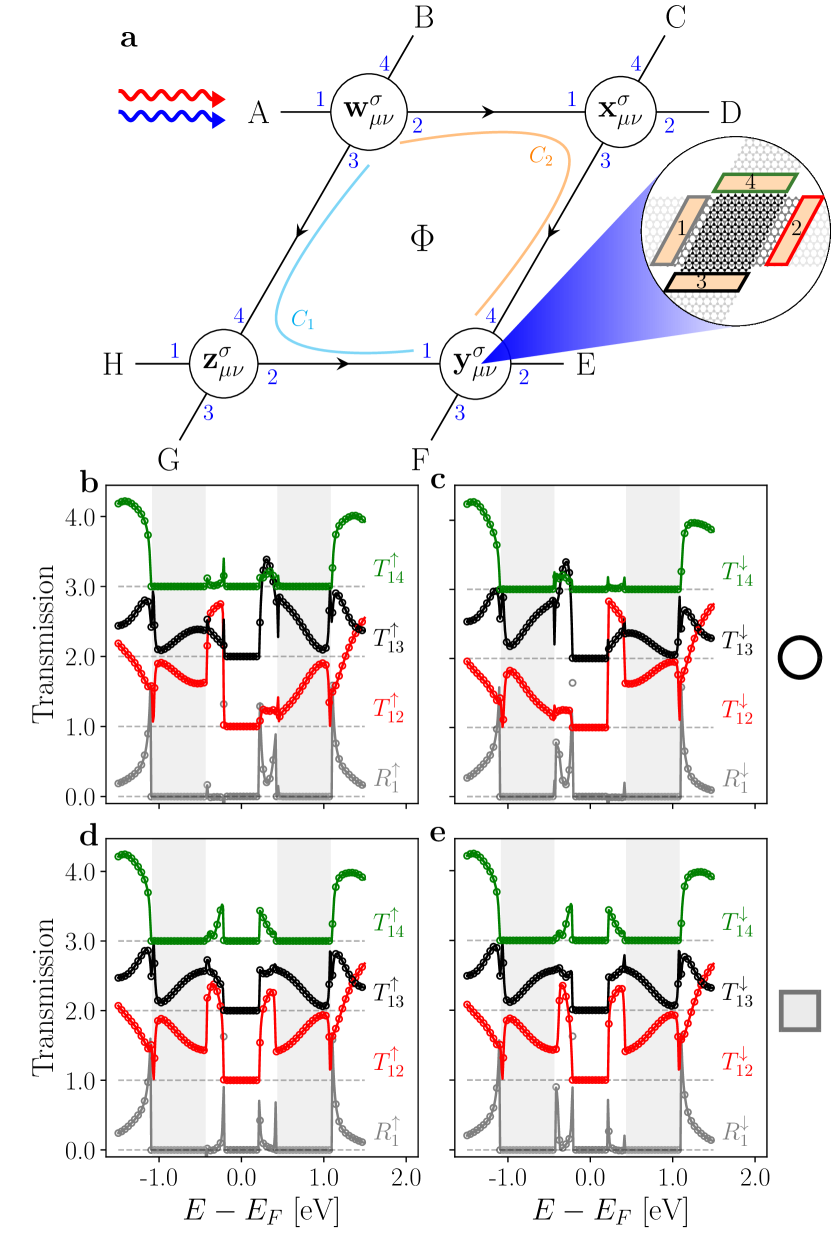
In figure 2(a) we sketch the eight-terminal interferometer as a composition of four independent scatterers represented by (lower-case), with , the S-matrix corresponding to each 4-terminal junction between two ZGNRs. Each junction can, in principle, have different spin configurations, as shown in figure 1(b). In figure 2(b,c) we show the transmission probabilities for a single crossing with spin configuration indicated with a circle in figure 1(b) for spin , respectively. Similarly, in figure 2(d,e) we show these results for a crossing with spin configuration sketched with a square in figure 1(b). Here we can observe that, on the one hand, there is no transmission into port 4 in any of the crossings (green curves) and no reflection (gray curves) in the single channel energy region (shaded area). On the other hand, by looking at figure 2(b-e) we can see that and are spin-dependent quantities (spin-polarizing beam splitter) for the crossing with spin configuration represented by a circle, while in the case of the crossing with spin configuration represented by a square, these transmission probabilities are spin independent (non-polarizing junction). For instance, by comparing figure 2(b) and (c) it can be seen that for eV. For this system, we find that the polarizing crossing displays a maximum spin polarization in the transmission probability (within the single-channel energy region) of around close to eV, for and . Similar results were found for a crossing of slightly narrower GNRs (8-ZGNRs) in Rref. [37]. Note that here we compare two methods to obtain the transmission probabilities, the scattering matrix formalism (open circles) and the NEGF method as implemented in TBtrans [60] (solid lines), which give essentially the same result.
The S-matrix of the complete interferometer, (uppercase), can then be written in terms of with appropriate connection of in- and outgoing electrode indices (). For electrons injected in the device from terminal A, one has:
| (12a) | |||||
| (12b) | |||||
| (12c) | |||||
| (12d) | |||||
| (12e) | |||||
| (12f) | |||||
| (12g) | |||||
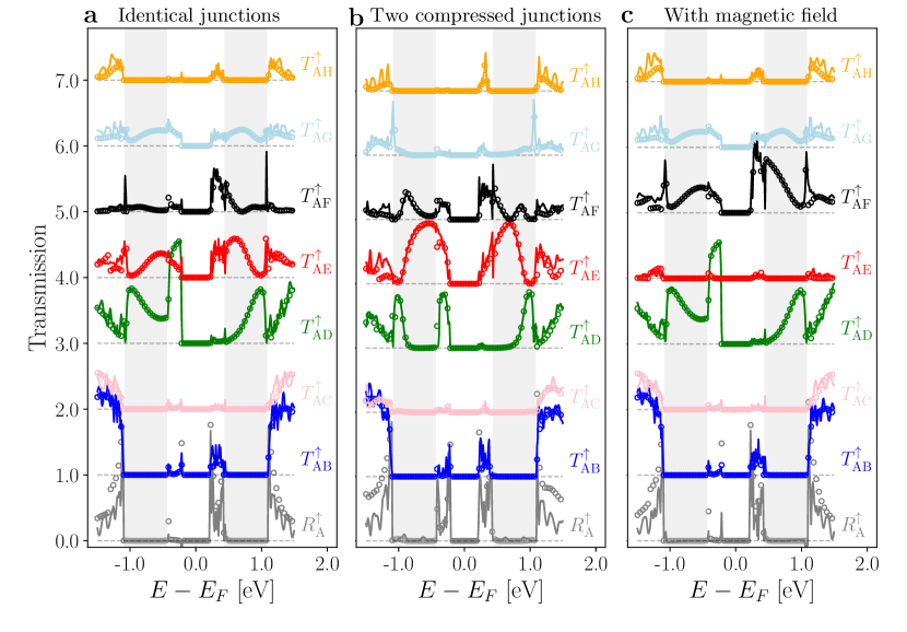
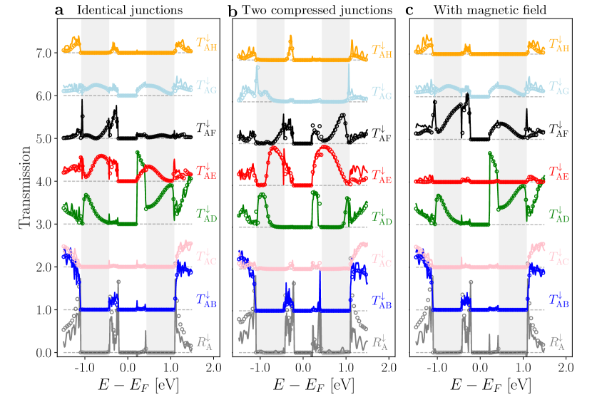
To test our approximation, we compare in figure 3(a) the transmission probabilities obtained with TBtrans [60] (solid lines) for the whole interferometer, with those obtained with the independent-scatterers approximation (open circles) using (12a)-(12g)). As shown in this panel, within the single-mode energy region (shaded areas), the approximation of independent scatterers yields a perfect overlap with the full solution. This is due to the lack of reflection and/or interband scattering in the ZGNRs junctions for electrons in the single-mode energy region, as shown in figure 2(b-e). In fact, for larger energies, the approximate (open circles) and full solution (solid lines) start to deviate, since here one should also take into account the contribution of the reflected beams between independent scatterers to coherently combine the scattering matrices of the junctions. For completeness, we performed the same analysis shown in figure 3 for electrons with the opposite spin , in figure 4. It can be seen that the same observations listed above hold for the other spin component.
3.2 Deviations from standard Mach-Zehnder setup
We note that in the ideal MZI interferometer two of the junctions should act as 50:50 electron beam splitters while the other two should act as perfect mirrors (where the outgoing electrons are transmitted with zero probability through those output ports). In other words, the only non-zero transmission probabilities should be and with (at the single-mode energy range). While in figure 3(a) we can observe that and , one could achieve the ideal MZI interferometer by forcing junctions and (considering an electron incoming from terminal A) to work as mirrors instead of beam splitters. One way to change the inter-/intra-ribbon transmission ratio (quantity that controls the performance of the junction) is by modifying the distance between the on-top and bottom ribbons (see figure 1) for such junctions. For instance, if the vertical distance between the ribbons is reduced, the transmission between them can be enhanced up to values close to (condition for a perfect mirror where the electron beam is fully transferred between the ribbons) [34].
In figure 3(b) we calculated the transmission probabilities using our independent-scatterers approximation with (12a)-(12g), where the scattering matrices and here correspond to a junction between two 10-ZGNRs with a relative distance that is reduced with respect to the junctions and ( Å versus Å). All junctions have the same spin configuration. In this figure we can observe that there is an energy range (for , approximately) where all except for and (ideal MZI).
Note that even in this scenario where the geometry of the interferometer has been distorted, the reflection probability still remains close to zero in the single-mode energy region (gray curves in figure 3(b)).
3.3 Magnetic-field dependence of scattering matrices
In presence of a magnetic field perpendicular to the interferometer plane (parallel to the -axis in this case), as the crossed ZGNRs enclose an area, there will be a magnetic flux encompassed by the ribbons (represented by in figure 2). Under these circumstances, the transmission probabilities between certain pairs of incoming/outgoing ports will be affected by the presence of the magnetic flux, as the electron injected can acquire a phase () by following certain paths that surround a region with non-zero vector potential enclosed by the interferometer,
| (12m) |
Here is the flux of an external magnetic field through the area enclosed by the contour (see figure 2). Because the global phase is arbitrary we can split the phase difference into contributions for the two pathways.
From (12a)-(12g) we observe that electrons incoming from terminal A only display interference for the pathways into terminals E and F, since here the S-matrices are built from a sum of two paths, as sketched in figure 2. To compute the transmission probabilities using the independent-scattering approximation, including the the additional phase contribution due to the presence of the magnetic field, we use the modified equations
| (12na) | |||||
| (12nb) | |||||
The corresponding transmission probabilities between these terminals show a periodic dependency on the magnetic flux as a result of the interference term between the two possible paths.
We only show calculations for the spin configuration 1 because the self-interference patterns are very similar for all spin configurations shown in figure 1(b). We note, however, that the spin polarization of the outgoing electron beam will depend on the chosen spin configuration. For instance, the spin-polarizing effect is absent for configuration 4 in the case where the geometry is perfectly symmetrical. Nevertheless, it is worth mentioning that away from the crossing angle of 60∘ (likely situation when building this geometry experimentally), each four-terminal junction generally polarizes the outgoing beam independently from the spin configuration [37].
To test how our approximation works with the magnetic field, we compare in figure 3(c) the transmission probabilities obtained with TBtrans [60] (solid lines) for the whole interferometer, with those obtained with the independent-scatterers approximation (open circles) when for a device with equal junctions, where Å. We choose such magnetic flux since it leads to a phase difference of , and thus to a complete extinction in one arm. The solid lines plotted in this panel were computed using the Peierls substitution (explained in section 2) with a magnetic field of T for the device of figure 1, of area nm2.
As shown in figure 3, in the single-mode energy region (shaded areas), the approximation of independent scatterers (open circles) also yields a perfect overlap with the full solution (solid lines) in presence of a transverse magnetic field.
Another important result seen in figure 3 is that the reflection probability is zero in the single-mode energy region both in presence or absence of a magnetic flux. Moreover, we also observe, as predicted, that the transmission probabilities that do not involve two possible paths (i.e., ) are insensitive to the magnetic field since the only curves that are affected by are and .
3.4 Self-interference pattern with magnetic field
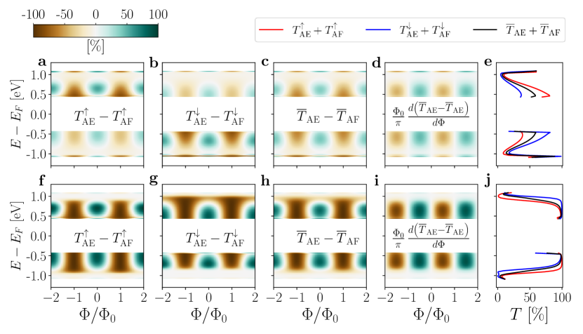
In figure 5 we show the interference patterns per spin channel of an interferometer by computing the transmission probability as a function of the incoming electron energy only in the single-mode energy window and for a magnetic flux . Only the single-band energy region is shown for which the independent-scatterers approximation provides accurate results. We plot the difference for in figure 5(a,b) and its average in figure 5(c). In figure 5(d) we plot the difference between the derivatives of the transmission probabilities and with respect to the magnetic flux. In this panel we can identify the regions of high sensitivity of the device. In figure 5(e) we plot the sum of the transmission probabilities for and its average per spin channel. While figure 5(a-e) correspond to a device formed of four equal junctions, figure 5(f-j) show a similar analysis for the ideal MZI where junctions and are compressed ( Å) to provide effective mirrors. The figure clearly reveals the AB effect for electrons after self-interfering in the outgoing terminals. We also see that the transmission probability is highly dependent on the electron energy and magnetic flux. These transmission probabilities also display a slight dependency on the spin index of the electrons, as the junctions in configuration 1 polarize the outgoing electron beam [37]. By comparing figure 5(a-e) to figure 5(f-j) we observe that the device with compressed junctions acts as an ideal MZI where the electron beam is transmitted only into ports E and F without losses, as the corresponding transmission probabilities in this case reach values close to 100%, while in the case of four equal junctions and reach maximum values of %. Note that the sum of the transmission probabilities shown in figure 5(e,j) is constant with respect to the magnetic flux, since the magnetic field only modifies the relative phase acquired by an electron between the two paths that interfere, but this phase does not change the transmission probabilities between electrode A and electrodes B, C, D, G, and H. Since the current must be conserved, while and are individually affected by the presence of the magnetic field, the sum of them must remain constant. As shown in figure 3(c), the complete extinction of the transmission into one arm is independent of the transmission ratio between the ZGNRs of junctions w and y (as long as they are identical), while the contrast of the signal shown in figure 5 is highly dependent on this ratio (and is optimal for 50:50 beam splitters).
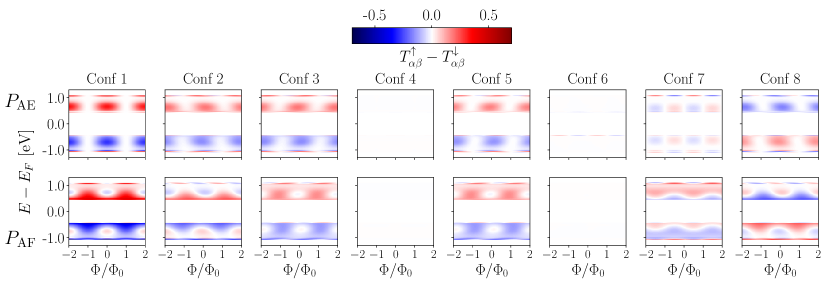
For completeness, in figure 6 we show the degree of transport spin polarization for the 8 possible spin configurations of figure 1(b), defined as
| (12no) |
We observe that the device’s spin configuration is not particularly relevant for the interference pattern, as the interference is determined by a periodic dependency on the magnetic flux. However, the spin configuration is important for controlling the spin polarization of the outgoing electron beam. Interestingly, we observe that the spin polarization not only varies with the electron energy, but can actually be tuned with the magnetic field. But we also see that there are certain spin configurations that do not give a polarized outgoing beam (such as configurations 4 and 6). In the case of configuration 4, it is easy to understand that the outgoing beam is not spin polarized as the four junctions in this case are non-polarizing [37]. In the case of configuration 6, while there are two spin-polarizing junctions (x and z), the one in the outgoing junction y is the spin-inverted version of the one in the incoming junction w. The multiplication of the corresponding scattering matrices results in a non-polarized outgoing beam.
3.5 Other applications
The MZI can be used to detect differential phase shifts between the two arms of the MZI, that could be caused, e.g., by defects, potentials in one of the four arms, path length, or by the charging state of nearby defects.
The functioning of the MZI depends crucially on the phase coherence of the electronic wave functions traveling along the two paths. Thus, it is natural that the MZI can also be used to detect decoherence and measure, e.g., the electron’s coherence length and how it is influenced by parameters such as temperature [65, 41, 39]. Furthermore, the MZI can be used to learn about properties of the carriers producing the signal, e.g., to measure the degree of indistinguishability of electrons [8, 9], or the statistics of the charge carriers in the device [38].
There are also several applications related to quantum information processing. The MZI can be used to implement single-qubit rotations (on charge qubits, or with spin-dependent phases induced, e.g., by spin-orbit interaction also for spin qubits), or to perform entangling operations such as parity measurements [66] or probabilistic entanglement generation [40].
Since the consideration of electron-electron interaction, spin-orbit interaction and decoherence is beyond the scope of this article, we will illustrate the use of the proposed GNR-MZI for phase detection.
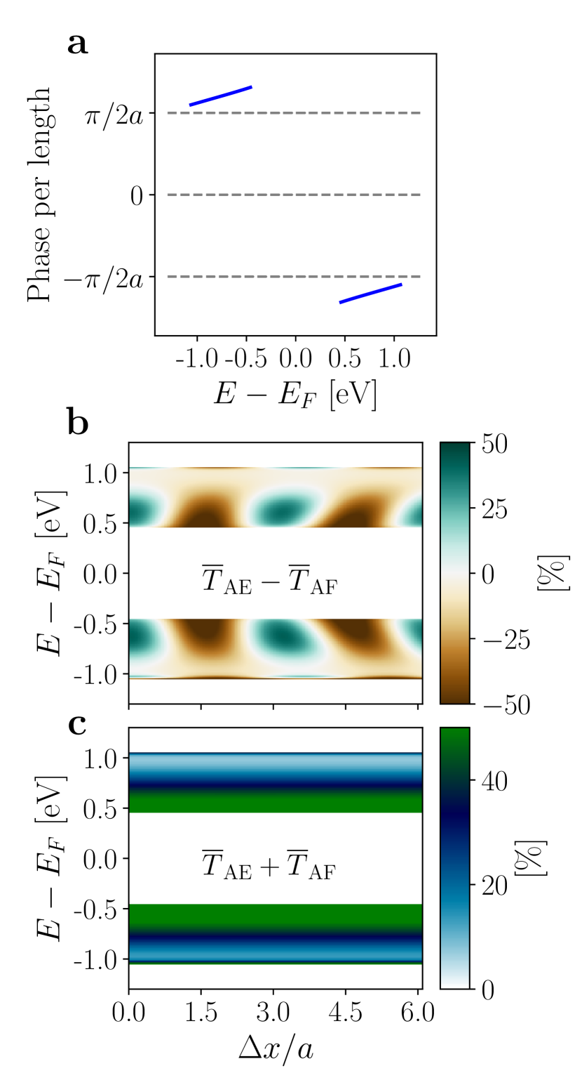
As an example, here we consider the case of a geometrical distortion where the length of one of the paths () is longer than the other () that could be caused, e.g., by the presence of a fold in one of the ribbons composing it or a corrugation in the substrate underneath. To simulate the presence of such geometrical distortion we include a section of a perfect ribbon between two ports to simulate the extra distance between the two paths. We do not consider any modified hopping or on-site energy terms in the Hamiltonian, as a first approximation.
Electrons propagating through the perfect ribbon section are transmitted with 100% probability. However, they acquire a phase that depends on the size of such section, which can be determined by computing the complex part of the transmission amplitude (scattering matrix) of this system. In the single-mode energy region this phase is easily determined since the scattering matrix of this section is of size . For this reason we can compute the overall scattering matrix of the interferometer by using the modified (12d) and (12e):
| (12npa) | |||||
| (12npb) | |||||
where, is the electronic phase shift per length unit of a perfect 10-ZGNR section, and represents the relative length difference between and . For this example we assume a longer distance between ports and , making the path Å longer than . Although other S-matrix elements of (12a)-(12g) are modified as well by the presence of such geometrical distortions (as, e.g., (12b) and (12c) considering that the section of a perfect 10-ZGNR is situated between junctions and ), the transmission probabilities associated to those matrices are not affected since a global phase does not change these values. However, in the case of (12d)-(12e), the presence of the 10-ZGNR section adds a relative phase between the two paths which affects the overall transmission probabilities associated to those S-matrices.
In figure 7(a) we plot the phase-shift per unit length acquired by an electron passing through a section of a perfect 10-ZGNR within the single-mode energy window. In figure 7(b,c) we plot difference and sum, respectively, of the average transmission probabilities and as a function of the relative length difference between and (), and the electron energy (only shown the single-mode energy range) in absence of an external magnetic field. Here it is easy to see that the interference pattern will also depend on these kind of geometrical distortions that affect the relative phase acquired by an electron after travelling through paths and .
4 Conclusions
In this work we have studied the performance of a device formed of four crossed ZGNRs as an electron and spin interferometer. As ZGNRs host spin-polarized states due to the presence of electron interactions, we use the mean-field Hubbard Hamiltonian to describe the spin physics in this device by including the Coulomb repulsion term. To solve the Schrödinger equation in each iteration step we use the NEGF formalism for this open quantum system. Since the junctions create spin-polarizing scattering potentials [37], the resulting transmitted electrons in the different outgoing directions are spin polarized as well.
Furthermore, since electrons are transmitted without reflection, we can consider the system as an array of independent scatterers by using the S-matrix of each 4-terminal junction and combining them correspondingly to compute the overall S-matrix for the full device. The agreement between this approximation and the full solution is practically exact in the single-channel energy region, where the backscattering and transmission into the other output are zero.
Since some of the output ports can be reached following two possible paths, the transmission probability into these depends on the self-interference of the propagating electron. Moreover, the self-interference pattern can be further tuned by applying an external uniform magnetic field as a consequence of the Aharonov–Bohm effect. Interestingly, the self-interference pattern will depend not only on the electron energy and magnetic flux, but also on the spin index of the transmitted electrons. To further analyze this effect, we also calculated the spin polarization in the transmission probability of the two outgoing directions of interest, as a function of the electron energy and magnetic flux. While in the case of the interference pattern, the spin configuration is not particularly relevant, as the interference is dominantly determined by the cosine dependency of the magnetic flux, the spin configuration will determine the spin polarization of the outgoing electron beam in the possible outgoing ports. For instance, depending on the combination of the spin configurations of the junctions, the resulting outgoing beam will be polarized or non-polarized. Remarkably, the spin polarization not only varies with the electron energy, it can also be tuned by the existing magnetic flux.
Since the invention and further development of the single-electron source [67], performing electron-quantum-optics experiments at the single-particle level is now possible, where both emission and detection achieve efficiencies that reach values even larger than photon-based sources [68]. While the major obstacle for quantum implementations with single flying electrons is decoherence, here we propose a graphene-based interferometer in which spin-orbit and hyperfine interaction—the two major intrinsic sources of spin relaxation and decoherence in GaAs devices—are expected to be small due to carbon’s low atomic mass and low abundance of spinful nuclei. In fact, realizing a MZI in GNR-based nanostructures would set the stage for electron quantum optics experiments in this platform and provide evidence for its viability as a basis for quantum computing.
Acknowledgements
We acknowledge fruitful discussions about the scattering matrix formalism with Pedro Brandimarte and Alexandre Reily Rocha. This work was funded by the Spanish MCIN/AEI/ 10.13039/501100011033 (PID2020-115406GB-I00 and PID2019-107338RB-C66), the Basque Department of Education (PIBA-2020-1-0014), the University of the Basque Country (UPV/EHU) through Grant IT-1569-22, and the European Union’s Horizon 2020 (FET-Open project SPRING Grant No. 863098).
References
References
- [1] Ji Y, Chung Y, Sprinzak D, Heiblum M, Mahalu D and Shtrikman H 2003 An electronic Mach–Zehnder interferometer Nature 422 415–418
- [2] Roulleau P, Portier F, Glattli D C, Roche P, Cavanna A, Faini G, Gennser U and Mailly D 2007 Finite bias visibility of the electronic Mach–Zehnder interferometer Phys. Rev. B 76(16) 161309
- [3] Zhang Y, McClure D T, Levenson-Falk E M, Marcus C M, Pfeiffer L N and West K W 2009 Distinct signatures for coulomb blockade and Aharonov–Bohm interference in electronic fabry-perot interferometers Phys. Rev. B 79(24) 241304
- [4] McClure D T, Zhang Y, Rosenow B, Levenson-Falk E M, Marcus C M, Pfeiffer L N and West K W 2009 Edge-state velocity and coherence in a quantum Hall Fabry-Pérot interferometer Phys. Rev. Lett. 103(20) 206806
- [5] Carbonell-Sanromà E, Brandimarte P, Balog R, Corso M, Kawai S, Garcia-Lekue A, Saito S, Yamaguchi S, Meyer E, Sánchez-Portal D and Pascual J I 2017 Quantum dots embedded in graphene nanoribbons by chemical substitution Nano Lett. 17 50–56
- [6] Henny M, Oberholzer S, Strunk C, Heinzel T, Ensslin K, Holland M and Schönenberger C 1999 The fermionic Hanbury Brown and Twiss experiment Science 284 296–298
- [7] Oliver W D, Kim J, Liu R C and Yamamoto Y 1999 Hanbury Brown and Twiss-type experiment with electrons Science 284 299–301
- [8] Samuelsson P, Sukhorukov E V and Büttiker M 2004 Two-particle Aharonov–Bohm effect and entanglement in the electronic Hanbury Brown–Twiss setup Phys. Rev. Lett. 92(2) 026805
- [9] Neder I, Ofek N, Chung Y, Heiblum M, Mahalu D and Umansky V 2007 Interference between two indistinguishable electrons from independent sources Nature 448 333–337
- [10] Splettstoesser J, Samuelsson P, Moskalets M and Büttiker M 2010 Two-particle Aharonov–Bohm effect in electronic interferometers J. Phys. A: Math. Theor. 43 354027
- [11] Castro Neto A H, Guinea F, Peres N M R, Novoselov K S and Geim A K 2009 The electronic properties of graphene Rev. Mod. Phys. 81(1) 109–162
- [12] Rickhaus P, Makk P, Liu M H, Tóvári E, Weiss M, Maurand R, Richter K and Schönenberger C 2015 Snake trajectories in ultraclean graphene junctions Nat. Commun. 6 6470
- [13] Chen S, Han Z, Elahi M M, Habib K M M, Wang L, Wen B, Gao Y, Taniguchi T, Watanabe K, Hone J, Ghosh A W and Dean C R 2016 Electron optics with - junctions in ballistic graphene Science 353 1522–1525
- [14] Son Y W, Cohen M L and Louie S G 2006 Half-metallic graphene nanoribbons Nature (London) 444 347–349
- [15] Son Y W, Cohen M L and Louie S G 2006 Energy gaps in graphene nanoribbons Phys. Rev. Lett. 97(21) 216803
- [16] Minke S, Bundesmann J, Weiss D and Eroms J 2012 Phase coherent transport in graphene nanoribbons and graphene nanoribbon arrays Phys. Rev. B 86(15) 155403
- [17] Baringhaus J, Ruan M, Edler F, Tejeda A, Sicot M, Taleb-Ibrahimi A, Li A P, Jiang Z, Conrad E H, Berger C, Tegenkamp C and de Heer W A 2014 Exceptional ballistic transport in epitaxial graphene nanoribbons Nature 506 349
- [18] Aprojanz J, Power S R, Bampoulis P, Roche S, Jauho A P, Zandvliet H J W, Zakharov A A and Tegenkamp C 2018 Ballistic tracks in graphene nanoribbons Nat. Commun. 9 4426
- [19] Zârbo L P and Nikolić B K 2007 Spatial distribution of local currents of massless Dirac fermions in quantum transport through graphene nanoribbons Europhys. Lett. (EPL) 80 47001
- [20] Cai J, Ruffieux P, Jaafar R, Bieri M, Braun T, Blankenburg S, Muoth M, Seitsonen A P, Saleh M, Feng X, Mullen K and Fasel R 2010 Atomically precise bottom-up fabrication of graphene nanoribbons Nature (London) 466 470–473
- [21] Ruffieux P, Wang S, Yang B, Sánchez-Sánchez C, Liu J, Dienel T, Talirz L, Shinde P, Pignedoli C A, Passerone D, Dumslaff T, Feng X, Müllen K and Fasel R 2016 On-surface synthesis of graphene nanoribbons with zigzag edge topology Nature 531 489
- [22] Clair S and de Oteyza D G 2019 Controlling a chemical coupling reaction on a surface: Tools and strategies for on-surface synthesis Chem. Rev. 119 4717
- [23] de Oteyza D G and Frederiksen T 2022 Carbon-based nanostructures as a versatile platform for tunable -magnetism J. Phys.: Condens. Matter 34 443001
- [24] Koch M, Ample F, Joachim C and Grill L 2012 Voltage-dependent conductance of a single graphene nanoribbon Nat. Nanotechnol. 7 713–717
- [25] Kawai S, Benassi A, Gnecco E, Söde H, Pawlak R, Feng X, Müllen K, Passerone D, Pignedoli C A, Ruffieux P, Fasel R and Meyer E 2016 Superlubricity of graphene nanoribbons on gold surfaces Science 351 957–961
- [26] Wang D, Bao D L, Zheng Q, Wang C T, Wang S, Fan P, Mishra S, Tao L, Xiao Y, Huang L, Feng X, Müllen K, Zhang Y Y, Fasel R, Ruffieux P, Du S and Gao H J 2023 Twisted bilayer zigzag-graphene nanoribbon junctions with tunable edge states Nat. Commun. 14 1018
- [27] Areshkin D A and White C T 2007 Building blocks for integrated graphene circuits Nano Lett. 7 3253–3259
- [28] Jayasekera T and Mintmire J W 2007 Transport in multiterminal graphene nanodevices Nanotechnology 18 424033
- [29] Jiao L, Zhang L, Ding L, Liu J and Dai H 2010 Aligned graphene nanoribbons and crossbars from unzipped carbon nanotubes Nano Research 3 387–394
- [30] Cook B G, Dignard P and Varga K 2011 Calculation of electron transport in multiterminal systems using complex absorbing potentials Phys. Rev. B 83(20) 205105
- [31] Botello-Méndez A R, Cruz-Silva E, Romo-Herrera J M, López-Urías F, Terrones M, Sumpter B G, Terrones H, Charlier J C and Meunier V 2011 Quantum transport in graphene nanonetworks Nano Lett. 11 3058–3064
- [32] Brandimarte P, Engelund M, Papior N, Garcia-Lekue A, Frederiksen T and Sánchez-Portal D 2017 A tunable electronic beam splitter realized with crossed graphene nanoribbons J. Chem. Phys. 146 092318
- [33] Lima L R F, Hernández A R, Pinheiro F A and Lewenkopf C 2016 A 50/50 electronic beam splitter in graphene nanoribbons as a building block for electron optics J. Phys.: Condens. Matter 28 505303
- [34] Sanz S, Brandimarte P, Giedke G, Sánchez-Portal D and Frederiksen T 2020 Crossed graphene nanoribbons as beam splitters and mirrors for electron quantum optics Phys. Rev. B 102(3) 035436
- [35] Fujita M, Wakabayashi K, Nakada K and Kusakabe K 1996 Peculiar localized state at zigzag graphite edge J. Phys. Soc. Jpn. 65 1920–1923
- [36] Magda G Z, Jin X, Hagymási I, Vancsó P, Osváth Z, Nemes-Incze P, Hwang C, Biró L P and Tapasztó L 2014 Room-temperature magnetic order on zigzag edges of narrow graphene nanoribbons Nature (London) 514 608
- [37] Sanz S, Papior N, Giedke G, Sánchez-Portal D, Brandbyge M and Frederiksen T 2022 Spin-polarizing electron beam splitter from crossed graphene nanoribbons Phys. Rev. Lett. 129(3) 037701
- [38] Law K T, Feldman D E and Gefen Y 2006 Electronic Mach–Zehnder interferometer as a tool to probe fractional statistics Phys. Rev. B 74(4) 045319
- [39] Jo M, Lee J Y M, Assouline A, Brasseur P, Watanabe K, Taniguchi T, Roche P, Glattli D C, Kumada N, Parmentier F D, Sim H S and Roulleau P 2022 Scaling behavior of electron decoherence in a graphene Mach–Zehnder interferometer Nature Communications 13 5473
- [40] Signal A I and Zülicke U 2005 Tunable entanglement generation for mobile-electron spin qubits Appl. Phys. Lett. 87 102102
- [41] Haack G, Moskalets M, Splettstoesser J and Büttiker M 2011 Coherence of single-electron sources from Mach–Zehnder interferometry Phys. Rev. B 84(8) 081303
- [42] Vyshnevyy A A, Lebedev A V, Lesovik G B and Blatter G 2013 Two-particle entanglement in capacitively coupled Mach–Zehnder interferometers Phys. Rev. B 87(16) 165302
- [43] Yamamoto M, Takada S, Bäuerle C, Watanabe K, Wieck A D and Tarucha S 2012 Electrical control of a solid-state flying qubit Nat. Nanotechnol. 7 247–251
- [44] Aharonov Y and Bohm D 1959 Significance of electromagnetic potentials in the quantum theory Phys. Rev. 115(3) 485–491
- [45] Recher P, Trauzettel B, Rycerz A, Blanter Y M, Beenakker C W J and Morpurgo A F 2007 Aharonov–Bohm effect and broken valley degeneracy in graphene rings Phys. Rev. B 76(23) 235404
- [46] Schelter J, Recher P and Trauzettel B 2012 The Aharonov–-Bohm effect in graphene rings Solid State Commun. 152 1411–1419
- [47] Duca L, Li T, Reitter M, Bloch I, Schleier-Smith M and Schneider U 2015 An Aharonov–Bohm interferometer for determining Bloch band topology Science 347 288–292
- [48] Mreńca-Kolasińska A and Szafran B 2016 Lorentz force effects for graphene Aharonov–Bohm interferometers Phys. Rev. B 94(19) 195315
- [49] Russo S, Oostinga J B, Wehenkel D, Heersche H B, Sobhani S S, Vandersypen L M K and Morpurgo A F 2008 Observation of Aharonov–Bohm conductance oscillations in a graphene ring Phys. Rev. B 77(8) 085413
- [50] Mirzakhani M, Myoung N, Peeters F and Park H 2023 Electronic mach-zehnder interference in a bipolar hybrid monolayer-bilayer graphene junction Carbon 201 734–744
- [51] Wei D S, van der Sar T, Sanchez-Yamagishi J D, Watanabe K, Taniguchi T, Jarillo-Herrero P, Halperin B I and Yacoby A 2017 Mach–Zehnder interferometry using spin- and valley-polarized quantum hall edge states in graphene Sci. Adv. 3 e1700600
- [52] Sanz S, Papior N, Brandbyge M and Frederiksen T 2022 hubbard: v0.2.0 URL https://doi.org/10.5281/zenodo.4748765
- [53] Slater J C and Koster G F 1954 Simplified LCAO method for the periodic potential problem Phys. Rev. 94(6) 1498–1524
- [54] Trambly de Laissardière G, Mayou D and Magaud L 2010 Localization of Dirac electrons in rotated graphene bilayers Nano Lett. 10 804–808
- [55] Keldysh L V 1965 Diagram technique for nonequilibrium processes Sov. Phys. JETP 20 1018 [Zh. Eksp. Theor. Fiz. 47, 1515 (1964)]
- [56] Kadanoff L and Baym G 1962 Quantum Statistical Mechanics: Green’s Function Methods in Equilibrium and Nonequilibrium Problems Frontiers in physics: a lecture note and reprint series (W.A. Benjamin)
- [57] Peierls R 1933 Zur Theorie des Diamagnetismus von Leitungselektronen Zeitschrift für Physik 80 763–791
- [58] Landauer R 1957 Spatial variation of currents and fields due to localized scatterers in metallic conduction IBM J. Res. Dev. 1 223–231
- [59] Büttiker M, Imry Y, Landauer R and Pinhas S 1985 Generalized many-channel conductance formula with application to small rings Phys. Rev. B 31(10) 6207–6215
- [60] Papior N, Lorente N, Frederiksen T, García A and Brandbyge M 2017 Improvements on non-equilibrium and transport Green function techniques: The next-generation TranSIESTA Comp. Phys. Commun. 212 8–24
- [61] Fisher D S and Lee P A 1981 Relation between conductivity and transmission matrix Phys. Rev. B 23(12) 6851–6854
- [62] Sancho M P L, Sancho J M L, Sancho J M L and Rubio J 1985 Highly convergent schemes for the calculation of bulk and surface Green functions J. Phys. F: Met. Phys. 15 851–858
- [63] Papior N R sisl: v0.12.2 URL https://doi.org/10.5281/zenodo.597181
- [64] Cahay M, McLennan M and Datta S 1988 Conductance of an array of elastic scatterers: A scattering-matrix approach Phys. Rev. B 37(17) 10125–10136
- [65] Seelig G and Büttiker M 2001 Charge-fluctuation-induced dephasing in a gated mesoscopic interferometer Phys. Rev. B 64(24) 245313
- [66] Haack G, Förster H and Büttiker M 2010 Parity detection and entanglement with a Mach–Zehnder interferometer Phys. Rev. B 82(15) 155303
- [67] Fève G, Mahé A, Berroir J M, Kontos T, Plaçais B, Glattli D C, Cavanna A, Etienne B and Jin Y 2007 An on-demand coherent single-electron source Science 316 1169–1172
- [68] Edlbauer H, Wang J, Crozes T, Perrier P, Ouacel S, Geffroy C, Georgiou G, Chatzikyriakou E, Lacerda-Santos A, Waintal X, Glattli D C, Roulleau P, Nath J, Kataoka M, Splettstoesser J, Acciai M, da Silva Figueira M C, Öztas K, Trellakis A, Grange T, Yevtushenko O M, Birner S and Bäuerle C 2022 Semiconductor-based electron flying qubits: review on recent progress accelerated by numerical modelling EPJ Quantum Technology 9 21