Length-independent quantum transport through
topological band states of graphene nanoribbons
In the realm of molecular electronics the active elements of an electronic device are composed of individual molecules McCreery et al. (2013); Metzger (2015); Xiang et al. (2016). Among the requested components in this field, a substantial effort has been devoted to the design of linear organic systems, often referred to as molecular wires, capable of transporting large electrical currents with negligible losses over long distances. Despite many efforts from communities working either at room temperature in liquid environments Xu and Tao (2003); Tuccitto et al. (2009); Kolivoška et al. (2013); Carini et al. (2017); Yao et al. (2020); Li et al. (2022); Lee et al. (2021) or at low temperature in ultra-high vacuum Lafferentz et al. (2009); Reecht et al. (2014, 2015); Nacci et al. (2015); Skidin et al. (2018), such a perfect molecular conductor has remained elusive. Graphene nanoribbons (GNRs), quasi-one-dimensional narrow strips of graphene, have emerged as promising candidates for high-performance molecular wires due to their extreme robustness inherited from graphene and their tunable energy band gaps resulting from lateral quantum confinement and edge effects Cai et al. (2010); Wang et al. (2021). In this framework, special attention has been paid to the topological properties of specifically designed GNRs in both theoretical and experimental studies Cao et al. (2017); Gröning et al. (2018); Rizzo et al. (2018, 2020). These exotic properties rely on specific edge modifications of the ribbons that may open a new way to optimize the transport efficiency of GNRs Koch et al. (2012); Jacobse et al. (2017, 2018); Lawrence et al. (2020); Mangnus et al. (2022); Friedrich et al. (2022). Here we present a systematic study of the charge transport properties of such topologically engineered GNRs, more specifically staggered edge-extended ribbons based on a 7-AGNR backbone denoted 7-AGNR-S(1,3) Gröning et al. (2018), using a low-temperature scanning tunneling microscopy (LT-STM) lifting procedure. Our experiments reveal (quasi-) lossless transport properties at low voltages with high conductance over long distances. These exceptional properties arise from charge transport channels between the modified ribbon edges and are due to low-energy electronic topological bands originating from coupled localized zero energy states. We thus realized a longstanding dream of molecular electronics: length-independent charge transport through a molecular conductor.
The transport properties of molecular wires were first investigated in solution, with molecular wires of increasing length bridging metallic electrodes Xu and Tao (2003); Su et al. (2016); Xin et al. (2019). In such an approach, the conductance–length relationship generally follows the simple exponential form , where is the wire length, is the contact conductance and , the inverse decay length which characterizes the intrinsic ability of the wire to transport the current Samanta et al. (1996); Khoo et al. (2015). The lower the value of , the more efficient is the transport of electrons through the wire. This approach was extensively used to probe soluble molecular wires, such as alkane or short conjugated structures, and has led, in a few cases, to values lower than 0.02 Å-1 Tuccitto et al. (2009); Kolivoška et al. (2013); Carini et al. (2017); Yao et al. (2020); Li et al. (2022); Lee et al. (2021). The recent development of on-surface synthesis (OSS) has considerably increased the types and lengths of molecular wires that can be probed Clair and de Oteyza (2019). Combined with LT-STM, it has led to a new type of experiment where the conductance of a given wire can be explored as a function of its length by progressively lifting the wire – with one end attached to the STM tip – from a metallic surface. The extremely well-controlled environment of this kind of experiment has allowed probing transport through defect-free wires several tens of nanometers long, and has revealed -0.4 Å-1 for conjugated polymers such as polyfluorene Lafferentz et al. (2009), polythiophene Reecht et al. (2014, 2015) and more complex donor-acceptor systems Nacci et al. (2015); Skidin et al. (2018). In this framework, GNRs have emerged as promising candidates for high-performance molecular wires Wang et al. (2021). Atomically precise fabrication of various types of GNRs has been achieved by OSS Cai et al. (2010); Narita et al. (2015) and revealed fascinating electronic Hao et al. (2020); Houtsma et al. (2021), magnetic Song et al. (2021), optical Chong et al. (2018); Miao et al. (2021), and mechanical Kawai et al. (2016); Koch et al. (2018) properties. Transport measurements with a 7-atom-wide armchair GNR (7-AGNR), the most conventional GNR with armchair edge structure, were reported early on, revealing Å-1 for low-voltage conditions and Å-1 at higher voltages corresponding to resonant conditions Koch et al. (2012); Jacobse et al. (2018). As such, the transport properties of 7-AGNRs are not significantly better than those of conjugated polymers, an effect that can be associated to their large electronic band gap ( eV) Koch et al. (2012). Indeed, similar measurements on the quasi-metallic 5-AGNR revealed Å-1 even for low-voltage conditions Lawrence et al. (2020), and the transport properties of GNRs can be further tuned by mixing short 5- and 7-AGNR segments together Jacobse et al. (2017); Mangnus et al. (2022). Narrow GNRs doped with substitutional boron atoms have also been observed to exhibit a metallic response over up to 2.2 nm Friedrich et al. (2022). In the present study, we report on (nearly) lossless quantum transport through individual GNRs over long distances ( nm), corresponding to values two orders of magnitude lower than in previous studies ( Å-1), under low voltage condition (50 mV) while preserving and high conductance ( G0, where G S is the quantum of conductance).
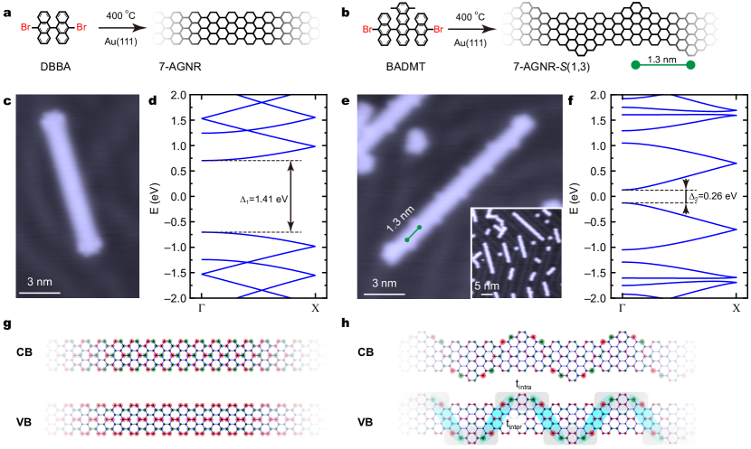
To that end, we investigated the edge-extended 7-AGNR-S(1,3)s Gröning et al. (2018) and compared it to the conventional 7-AGNRs Cai et al. (2010). Electronic transport through a lifted 7-AGNR has been explored thoroughly Koch et al. (2012); Jacobse et al. (2018) and is used here as a reference. These GNRs were assembled by OSS on Au(111) using 10,10’-dibromo-9,9’-bianthryl (DBBA, Figure 1a) Cai et al. (2010) and 6,11-bis(10-bromoanthracen-9-yl)-1,4-dimethyltetracene (BADMT, Figure 1b) Gröning et al. (2018) as precursors for 7-AGNRs and 7-AGNR-S(1,3)s, respectively. Figures 1c and 1e show typical STM images of these GNRs. The 7-AGNRs appear as featureless stripes with finger-like termini at small bias voltages (Figure 1c), consistent with previous reports Koch et al. (2012); Talirz et al. (2013). In contrast, the 7-AGNR-S(1,3)s reveal protrusions alternating on both sides of the backbone with a half-periodicity of 1.3 nm (Figure 1e). The strict alternation is due to steric effects during the polymerization procedure Gröning et al. (2018). As shown in the large-scale image (inset of Figure 1e), the maximum length of the 7-AGNR-S(1,3)s is approximately 20 nm, a limit that may be related to the typical dimensions of the Au(111) herringbone reconstruction Cai et al. (2010).
The electronic band structures from simple tight-binding (TB) calculations of 7-AGNRs and 7-AGNR-S(1,3)s, shown in Figure 1d and 1f, reveal band gaps of eV and eV, respectively, separating the valence band (VB) and conduction band (CB) states (Figure 1g for 7-AGNRs and Figure 1h for 7-AGNR-S(1,3)s). This substantial reduction of the band gap upon edge decoration plays an important role for electron transport through the ribbons. Additionally, in contrast to the 7-AGNRs, the VB and CB states of 7-AGNR-S(1,3)s are highly localized at the edge sites. As reported in Ref. Gröning et al., 2018 these low-energy bands can be rationalized from an SSH model with two hopping parameters along and across the backbone of nearly equal amplitude (tintra = 0.45 eV, tinter = 0.59 eV), resulting in a dispersive band with very small intrinsic band gap.
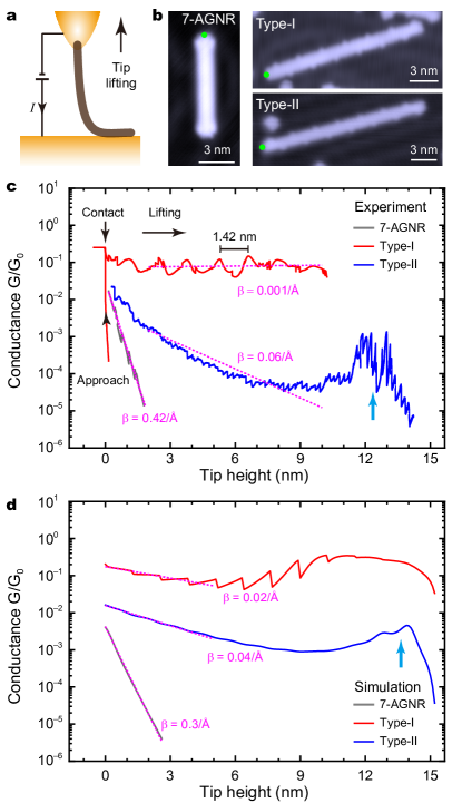
We now turn to the charge transport properties of both GNRs. The experimental procedure is sketched in Figure 2a. First, the STM tip is positioned above a terminus of a GNR with a low bias of mV (unless noted otherwise), then the tip is approached until a contact with the GNR – identified by a plateau in the conductance trace – is established, and eventually the tip is lifted vertically from the surface with the GNR attached to the tip apex with the current traversing the junction recorded simultaneously.
Typical conductance measurements for three OSS-fabricated GNRs, one 7-AGNR and two 7-AGNR-S(1,3)s (STM images in Figure 2b), are shown in Figure 2c. For the 7-AGNR, the retraction of the tip reveals an exponential conductance decrease (gray curve) with a decay constant of Å-1, consistent with previous reports Koch et al. (2012). Such a high value leads to a conductance lower than G0 for the ribbon lifted by only 2 nm, limiting the potential applications of 7-AGNRs in future electronic devices. In contrast, for the 7-AGNR-S(1,3)s we observed two distinct types of conductance behaviors as the tip is lifted, denoted Type-I (red) and Type-II (blue) in the following. Both types show remarkably high conductance at long lifting distances in comparison to that of 7-AGNRs.
The Type-I ribbon reported in Figure 2c (red curve) shows a near length-independent oscillatory conductance around a high value ( G0) with a periodicity of nm and an overall decay constant as low as Å-1. Some scattering around these values for other measured ribbons is reported in Supplementary Information (SI) Section 1. The conductance oscillation has an average periodicity very close (% larger) to the distance of nm separating successive units of the 7-AGNR-S(1,3) (Figure 1), suggesting that these conductance fluctuations reflect the detachment of successive units from the substrate surface Reecht et al. (2015).
The Type-II ribbon reported in Figure 2c (blue curve) follows a different behavior. The conductance decays smoothly over 6 to 7 nm before a plateau is reached at G0, leading to a conductance a thousand times smaller than the similar Type-I ribbon for a lifted distance of 9 nm. Surprisingly, the conductance of Type-II then increases again upon further lifting up to nm (which would correspond to ). Eventually, the conductance decreases again for distances close to the overall length of the ribbon nm. The conductance traces also reveal tiny but abrupt jerks with a periodicity of nm (detailed in SI Section 1), which matches well with the lattice constant of the Au(111) surface. A detailed analysis of STM images of several 7-AGNR-S(1,3) of Type-I and Type-II does not reveal an obvious difference in their structures or their adsorption configurations on the substrate, hinting towards an effect resulting from different connections between the STM-tip and the GNR-terminus.
Transport simulations based on an effective TB model can capture the qualitative features of the experiments as shown in Figure 2d. The 7-AGNR shows a characteristic decay of the conductance with suspended ribbon length due to the exponential decay of tunneling electrons in the energy range within the band gap. The 7-AGNR-S(1,3) on the other hand has a much smaller band gap which results in band states available much closer to the Fermi level of the electrodes, and therefore to a higher overall conductance. In fact, ballistic transport is obtained whenever a band state falls within the bias window. In line with the general trend that GNRs are slightly -doped on Au(111) Merino-Díez et al. (2017), which is supported by our DFT calculations (SI Section 2), the VB states are the ones aligned closest to and thus the ones involved in the electron transport process. Our model further enables us to reproduce the behaviour of both Type-I and Type-II ribbons by considering two different models for the molecular level alignment relative to as elaborated below.
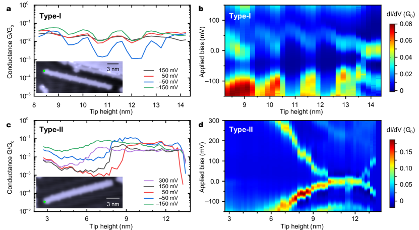
In order to understand the physics behind these different transport characteristics, both conductance () and differential conductance () spectra were acquired during a step-by-step lifting procedure with 0.2 nm step size. The conductance measurement of the Type-I ribbon (inset of Figure 3a) was performed with the tip retracting from 8.3 to 14.5 nm. Reconstructed from spectra acquired at discrete tip heights, the junction conductance at different voltages is represented in Figure 3a. Independently of the applied voltage, the junction conductance remains essentially constant around 0.02 G0, with the exception of a characteristic oscillation with a periodicity of 1.4 nm already reported in Figure 1c. The spectra acquired during the same lifting procedure (Figure 3b) reveal clear fingerprints of a transport resonance around the Fermi level and two others at V and V. Whereas these three resonances show nearly constant intensities with tip retraction, their positions fluctuate with a periodicity that matches the 1.4 nm oscillations in the conductance trace (Figure 3a). A simple analysis of these spectra assigns the nearly length-independent conductance of Type-I ribbons to the presence of at least one of these resonances within the bias window, whereas the conductance oscillations seem due to shifts of the voltage resonances that appear with the periodicity of the edge modifications in the GNRs.
In Figure 3c and 3d we summarize the similar investigations with a Type-II ribbon. In agreement with the data presented in Fig. 2c, the junction conductance is rather different from that of Type-I ribbons. Figure 3c reveals that, for all applied voltages, the junction conductance slowly decreases for short lifting distances before a sudden conductance increase is observed at lifting distances that depend on the applied voltage, i.e., the tip height onset occurs later at lower voltages. For short tip-sample separation ( nm), spectra recorded simultaneously do not reveal any spectral features in the probed voltage window ( V V), in agreement with the exponentially decaying conductance observed at the early stage of the retraction for Type-II. When the ribbon is lifted further ( nm), two resonances emerge (at and 0.25 V for nm). The voltage difference between these two peaks shrinks as the ribbon is further lifted, and eventually vanishes for nm. For nm the features split again, leaving the impression of two nearly parabolic dispersions. Beside these two spectral contributions, two other resonances briefly enter the bias windows (for 9 nm nm) and follow a similar parabolic dispersion. From these data we conclude that the conductance decrease observed at low -values corresponds to out-of-resonance transport conditions, whereas the conductance increase at 6 to 9 nm, and the following conductance plateau, mark the onset of resonant transport through band states that have shifted into the bias window.
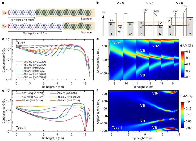
The experimental trends reported in Figure 3 are well captured by our model simulations. Figure 4a illustrates the transport setup for two different tip heights. The left side of the ribbon is chemically bonded to the tip electrode at the center carbon atom (gray site) at the terminal zigzag edge and electrons are considered to tunnel (with rate ) between the tip electrode and the nearby orbitals (red sites) that form part of the conjugated structure. Similarly, at the right side of the ribbon electrons are considered to tunnel (with rate ) between the substrate electrode and the orbitals directly above it (green sites). In other words, the tip height is modeled by varying the number of sites in contact with the substrate, with direct consequences for the electron transport between the electrodes.
Besides the tunnel couplings and , two more parameters are included in our simulation: the charge state of the GNR and the ratio of the voltage drops at the two electrode interfaces (tip-GNR and GNR-Au(111)). First, as sketched in Figure 4b, in equilibrium the VB and VB-1 states are aligned just below the Fermi level , consistent with the trend that GNRs on Au(111) typically result in -type doping Merino-Díez et al. (2017). Such level alignment is also corroborated by our DFT calculations reported in the SI Section 2. Secondly, when a voltage is applied, our model assumes an asymmetric potential profile with voltage drops of 1/3 and 2/3 over the two interfaces, respectively. A voltage drop over both interfaces implies that the VB resonances are seen in for both bias polarities Nazin et al. (2005).
In essence, length-independent transport is therefore observed whenever a VB state is accessible within the energy window given by the applied bias voltage (Figure 4b). Conversely, an exponentially decaying conductance trace is observed while the GNR states fall outside the bias window. As explained in SI Section 3, our interpretation of the difference between the experimentally observed Type-I and Type-II ribbons relies on the following physical mechanisms: (i) Type-I ribbons are considered to be strongly bound to the tip electrode such that most of the applied voltage drop occurs over the GNR-substrate interface (i.e., is tip and is substrate in Figure 4b). Further, the precise -doping level of the GNR is considered to be correlated with the detachment of each precursor unit. A possible origin of this may be related to subtle modifications of the GNR/substrate interface during the detachment, which in turn leads to conductance oscillations with a periodicity of nm. (ii) Type-II ribbons are considered to be weaker bound to the tip electrode such that most of the voltage drop occurs over the tip-GNR interface (i.e., is substrate and is tip in Figure 4b). The donation of charge is not considered to be significantly correlated with the liftoff process for Type-II, hence the absence of the conductance oscillations with a periodicity of nm as observed for Type-I. These considerations can qualitatively explain the experimental data as explained in the following.
Figure 4c and 4d report the simulated conductance and the differential conductance at different voltages for Type-I ribbons. Overall, the traces are characterized by length-independent transport from start to the end. At positive polarity the conductance is somewhat larger and the plateau more flat than at negative polarity. As in the experiment (Figure 3a), the oscillations are most pronounced at small voltages. The features observed in are fingerprints of the VB and VB-1 states that appear at both polarities (Figure 4b) due to voltage drops over both interfaces. The spacing is closer at the positive polarity because most of the voltage drop is assumed to occur over the GNR-substrate interface.
Figure 4e and 4f for Type-II ribbons, on the other hand, exhibit the initial phase of the liftoff process that is characterized by an exponential decrease of conductance due to the VB states aligned outside the transport bias window. However, as the GNR is gradually removed from the substrate, the molecular resonances narrow in energy (reduced substrate hybridization) and, consistent with our assumption of a constant -doping level, must therefore drift up in energy. This eventually brings the VB and VB-1 states inside the bias window and the conductance trace increases to reach a high-conductance plateau similar to Type-I. Again, the features observed in are fingerprints of the VB and VB-1 resonances that appear at both polarities due to a voltage drop over both interfaces. But contrary to Type-I, the spacing is now closer at the negative polarity because most of the voltage drop is assumed to occur over the tip-GNR interface.
In conclusion, we performed a systematic study of the transport properties of the edge-modified 7-AGNR-S(1,3) in a LT-STM liftoff procedure. These ribbons host electronic low-energy topological bands supported by zigzag-edge decorations. These topological bands are responsible for length-independent and efficient charge transport in the suspended GNR geometry. The transport behavior is highly sensitive to the coupling between the ribbon and the electrodes. Overall, the critical factor for high-conductance ballistic transport is related to the presence of delocalized valence band states within the bias window. Future studies may explore further the possible relationship between the topological nature of the band and the extraordinary transport characteristics of the 7-AGNR-S(1,3). Our approach opens a path to the realization of tunable molecular components based on the rational design of graphene nanoribbons edges.
Acknowledgements This project has received funding from the European Research Council (ERC) under the European Union’s Horizon 2020 research and innovation program (grant agreement No 771850). The International Center for Frontier Research in Chemistry (FRC) is also acknowledged for financial support. This research was supported by the Swiss National Science Foundation under Grant No. 200020_182015, the Werner Siemens Foundation (CarboQuant). TF acknowledges support by the Spanish MCIN/AEI/ 10.13039/501100011033 (PID2020-115406GB-I00), the Basque Department of Education (PIBA-2020-1-0014), and the European Union through Horizon 2020 (FET-Open project “SPRING” Grant no. 863098).K.M. acknowledges a fellowship from Gutenberg Research College Johannes Gutenberg University Mainz. R.F. thanks Oliver Gröning for stimulating discussions.
I Methods
The experiments were performed with a low-temperature ultrahigh-vacuum STM (Omicron) at a base pressure of torr at 4.6 K. Atomically flat Au(111) substrates were prepared via cycles of argon ion sputtering and annealing under ultrahigh vacuum conditions. Electrochemically etched W tips were covered with gold by repeated indentation into the substrate. On-surface synthesis of these GNRs was performed using 10,10’-dibromo-9,9’-bianthryl (DBBA, Figure 1a) Cai et al. (2010) and 6,11-bis(10-bromoanthracen-9-yl)-1,4-dimethyltetracene (BADMT, Figure 1b) Gröning et al. (2018) as precursors for 7-AGNRs and 7-AGNR-S(1,3)s, respectively. The precursors were sublimed onto freshly cleaned Au(111) substrates held at room temperature. The samples were then gradually annealed to 400 ℃, leading to the formation of the GNRs as detailed in previous studies Cai et al. (2010); Gröning et al. (2018). Differential conductance d/d spectra were recorded in constant-height mode (open feedback loop) with a voltage modulation of 20 mV and a modulation frequency of 901 Hz.
To simulate the electronic properties of suspended GNRs we adopted a transparent and simple description based on a nearest-neighbor TB model of the carbon orbitals with hopping matrix elements set to eV Papior (2022). The low-bias differential conductance as a function of the liftoff distance was simulated using Green’s function theory in the wide-band approximation for the tip and substrate electrodes as described in the SI. We ignore effects of curvature by considering a model as illustrated in Figure 4a. The tip apex atom is considered to form a strong chemical bond to the central carbon atom at the terminal zigzag edge, resulting in hybridization and thus in removal of the corresponding orbital from the conjugated network. The tip electrode is consequently considered to inject/extract electrons to/from the closest carbon sites (red disks) characterized by the tunneling rate . On the other hand, the number of atomic sites with coupling to the substrate electrode (green disks) is considered to be gradually reduced as a function of tip retraction from the surface. This numerically efficient description allowed us to explore a wide range of transport scenarios and possible effects, including different models for the potential drop across the GNR, deviations from charge neutrality, disorder, etc. Based on this exploration we found that the most suitable description for our experimental observations corresponds to a model in which the Fermi level is aligned close to the VB edge and where the current—at both bias polarities—involves propagation through a few VB states that fall within the transport energy window. Another key ingredient is the precise molecular level alignment relative to , which our modeling suggests to undergo small shifts as a function of the tip height due to changes in the electrode couplings. This enables a switching of the VB states in or out of the transport window. The key parameters and assumptions in our transport model are corroborated by DFT calculations for the electronic structure of a partly lifted 7-AGNR-S(1,3) on Au(111) as explained in the SI Section 2.
References
- McCreery et al. (2013) R. L. McCreery, H. Yan, and A. J. Bergren, “A critical perspective on molecular electronic junctions: there is plenty of room in the middle,” Phys. Chem. Chem. Phys. 15, 1065 (2013).
- Metzger (2015) R. M. Metzger, “Unimolecular electronics,” Chem. Rev. 115, 5056 (2015).
- Xiang et al. (2016) D. Xiang, X. Wang, C. Jia, T. Lee, and X. Guo, “Molecular-scale electronics: from concept to function,” Chem. Rev. 116, 4318 (2016).
- Xu and Tao (2003) B. Xu and N. J. Tao, “Measurement of single-molecule resistance by repeated formation of molecular junctions,” Science 301, 1221 (2003).
- Tuccitto et al. (2009) N. Tuccitto, V. Ferri, M. Cavazzini, S. Quici, G. Zhavnerko, A. Licciardello, and M. A. Rampi, “Highly conductive 40-nm-long molecular wires assembled by stepwise incorporation of metal centres,” Nat. Mater. 8, 41 (2009).
- Kolivoška et al. (2013) V. Kolivoška, M. Valášek, M. Gál, R. Sokolová, J. Bulickova, L. Pospisil, G. Mészáros, and M. Hromadová, “Single-molecule conductance in a series of extended viologen molecules,” J. Phys. Chem. Lett. 4, 589 (2013).
- Carini et al. (2017) M. Carini, M. P. Ruiz, I. Usabiaga, J. A. Fernández, E. J. Cocinero, M. Melle-Franco, I. Diez-Perez, and A. Mateo-Alonso, “High conductance values in -folded molecular junctions,” Nat. Commun. 8, 15195 (2017).
- Yao et al. (2020) X. Yao, X. Sun, F. Lafolet, and J.-C. Lacroix, “Long-range charge transport in diazonium-based single-molecule junctions,” Nano Lett. 20, 6899 (2020).
- Li et al. (2022) L. Li, J. Z. Low, J. Wilhelm, G. Liao, S. Gunasekaran, C. R. Prindle, R. L. Starr, D. Golze, C. Nuckolls, M. L. Steigerwald, et al., “Highly conducting single-molecule topological insulators based on mono- and di-radical cations,” Nat. Chem. (2022).
- Lee et al. (2021) H. J. Lee, S. J. Cho, H. Kang, X. He, and H. J. Yoon, “Achieving ultralow, zero, and inverted tunneling attenuation coefficients in molecular wires with extended conjugation,” Small 17, 2005711 (2021).
- Lafferentz et al. (2009) L. Lafferentz, F. Ample, H. Yu, S. Hecht, C. Joachim, and L. Grill, “Conductance of a single conjugated polymer as a continuous function of its length,” Science 323, 1193 (2009).
- Reecht et al. (2014) G. Reecht, F. Scheurer, V. Speisser, Y. J. Dappe, F. Mathevet, and G. Schull, “Electroluminescence of a polythiophene molecular wire suspended between a metallic surface and the tip of a scanning tunneling microscope,” Phys. Rev. Lett. 112, 047403 (2014).
- Reecht et al. (2015) G. Reecht, H. Bulou, F. Scheurer, V. Speisser, F. Mathevet, C. González, Y. J. Dappe, and G. Schull, “Pulling and stretching a molecular wire to tune its conductance,” J. Phys. Chem. Lett. 6, 2987 (2015).
- Nacci et al. (2015) C. Nacci, F. Ample, D. Bleger, S. Hecht, C. Joachim, and L. Grill, “Conductance of a single flexible molecular wire composed of alternating donor and acceptor units,” Nat. Commun. 6, 7397 (2015).
- Skidin et al. (2018) D. Skidin, T. Erdmann, S. Nikipar, F. Eisenhut, J. Krüger, F. Günther, S. Gemming, A. Kiriy, B. Voit, D. A. Ryndyk, et al., “Tuning the conductance of a molecular wire by the interplay of donor and acceptor units,” Nanoscale 10, 17131 (2018).
- Cai et al. (2010) J. Cai, P. Ruffieux, R. Jaafar, M. Bieri, T. Braun, S. Blankenburg, M. Muoth, A. P. Seitsonen, M. Saleh, X. Feng, et al., “Atomically precise bottom-up fabrication of graphene nanoribbons,” Nature 466, 470 (2010).
- Wang et al. (2021) H. Wang, H. S. Wang, C. Ma, L. Chen, C. Jiang, C. Chen, X. Xie, A.-P. Li, and X. Wang, “Graphene nanoribbons for quantum electronics,” Nat. Rev. Phys. 3, 791 (2021).
- Cao et al. (2017) T. Cao, F. Zhao, and S. G. Louie, “Topological phases in graphene nanoribbons: junction states, spin centers, and quantum spin chains,” Phys. Rev. Lett. 119, 076401 (2017).
- Gröning et al. (2018) O. Gröning, S. Wang, X. Yao, C. A. Pignedoli, G. B. Barin, C. Daniels, A. Cupo, V. Meunier, X. Feng, A. Narita, et al., “Engineering of robust topological quantum phases in graphene nanoribbons,” Nature 560, 209 (2018).
- Rizzo et al. (2018) D. J. Rizzo, G. Veber, T. Cao, C. Bronner, T. Chen, F. Zhao, H. Rodriguez, S. G. Louie, M. F. Crommie, and F. R. Fischer, “Topological band engineering of graphene nanoribbons,” Nature 560, 204 (2018).
- Rizzo et al. (2020) D. J. Rizzo, G. Veber, J. Jiang, R. McCurdy, T. Cao, C. Bronner, T. Chen, S. G. Louie, F. R. Fischer, and M. F. Crommie, “Inducing metallicity in graphene nanoribbons via zero-mode superlattices,” Science 369, 1597 (2020).
- Koch et al. (2012) M. Koch, F. Ample, C. Joachim, and L. Grill, “Voltage-dependent conductance of a single graphene nanoribbon,” Nat. Nanotechnol. 7, 713 (2012).
- Jacobse et al. (2017) P. H. Jacobse, A. Kimouche, T. Gebraad, M. Ervasti, J. Thijssen, P. Liljeroth, and I. Swart, “Electronic components embedded in a single graphene nanoribbon,” Nat. Commun. 8, 119 (2017).
- Jacobse et al. (2018) P. H. Jacobse, M. J. Mangnus, S. J. Zevenhuizen, and I. Swart, “Mapping the conductance of electronically decoupled graphene nanoribbons,” ACS Nano 12, 7048 (2018).
- Lawrence et al. (2020) J. Lawrence, P. Brandimarte, A. Berdonces-Layunta, M. S. Mohammed, A. Grewal, C. C. Leon, D. Sanchez-Portal, and D. G. de Oteyza, “Probing the magnetism of topological end states in 5-armchair graphene nanoribbons,” ACS Nano 14, 4499 (2020).
- Mangnus et al. (2022) M. J. J. Mangnus, F. R. Fischer, M. F. Crommie, I. Swart, and P. H. Jacobse, “Charge transport in topological graphene nanoribbons and nanoribbon heterostructures,” Phys. Rev. B 105, 115424 (2022).
- Friedrich et al. (2022) N. Friedrich, R. E. Menchon, I. Pozo, J. Hieulle, A. Vegliante, J. Li, D. Sanchez-Portal, D. Pena, A. Garcia-Lekue, and J. I. Pascual, “Addressing electron spins embedded in metallic graphene nanoribbons,” arXiv:2206.07583v1 (2022).
- Su et al. (2016) T. A. Su, M. Neupane, M. L. Steigerwald, L. Venkataraman, and C. Nuckolls, “Chemical principles of single-molecule electronics,” Nat. Rev. Mater. 1, 16002 (2016).
- Xin et al. (2019) N. Xin, J. Guan, C. Zhou, X. Chen, C. Gu, Y. Li, M. A. Ratner, A. Nitzan, J. F. Stoddart, and X. Guo, “Concepts in the design and engineering of single-molecule electronic devices,” Nat. Rev. Phys. 1, 211 (2019).
- Samanta et al. (1996) M. P. Samanta, W. Tian, S. Datta, J. I. Henderson, and C. P. Kubiak, “Electronic conduction through organic molecules,” Phys. Rev. B 53, R7626 (1996).
- Khoo et al. (2015) K. H. Khoo, Y. Chen, S. Li, and S. Y. Quek, “Length dependence of electron transport through molecular wires – a first principles perspective,” Phys. Chem. Chem. Phys. 17, 77 (2015).
- Clair and de Oteyza (2019) S. Clair and D. G. de Oteyza, “Controlling a chemical coupling reaction on a surface: tools and strategies for on-surface synthesis,” Chem. Rev. 119, 4717 (2019).
- Narita et al. (2015) A. Narita, X.-Y. Wang, X. Feng, and K. Müllen, “New advances in nanographene chemistry,” Chem. Soc. Rev. 44, 6616 (2015).
- Hao et al. (2020) Z. Hao, H. Zhang, Z. Ruan, C. Yan, J. Lu, and J. Cai, “Tuning the electronic properties of atomically precise graphene nanoribbons by bottom-up fabrication,” ChemNanoMat 6, 493 (2020).
- Houtsma et al. (2021) R. S. K. Houtsma, J. de la Rie, and M. Stöhr, “Atomically precise graphene nanoribbons: interplay of structural and electronic properties,” Chem. Soc. Rev. 50, 6541 (2021).
- Song et al. (2021) S. Song, J. Su, M. Telychko, J. Li, G. Li, Y. Li, C. Su, J. Wu, and J. Lu, “On-surface synthesis of graphene nanostructures with -magnetism,” Chem. Soc. Rev. 50, 3238 (2021).
- Chong et al. (2018) M. C. Chong, N. Afshar-Imani, F. Scheurer, C. Cardoso, A. Ferretti, D. Prezzi, and G. Schull, “Bright electroluminescence from single graphene nanoribbon junctions,” Nano Lett. 18, 175 (2018).
- Miao et al. (2021) W. Miao, L. Wang, X. Mu, and J. Wang, “The magical photoelectric and optoelectronic properties of graphene nanoribbons and their applications,” J. Mater. Chem. C 9, 13600 (2021).
- Kawai et al. (2016) S. Kawai, A. Benassi, E. Gnecco, H. Söde, R. Pawlak, X. Feng, K. Müllen, D. Passerone, C. A. Pignedoli, P. Ruffieux, et al., “Superlubricity of graphene nanoribbons on gold surfaces,” Science 351, 957 (2016).
- Koch et al. (2018) M. Koch, Z. Li, C. Nacci, T. Kumagai, I. Franco, and L. Grill, “How structural defects affect the mechanical and electrical properties of single molecular wires,” Phys. Rev. Lett. 121, 047701 (2018).
- Talirz et al. (2013) L. Talirz, H. Söde, J. Cai, P. Ruffieux, S. Blankenburg, R. Jafaar, R. Berger, X. Feng, K. Müllen, D. Passerone, et al., “Termini of bottom-up fabricated graphene nanoribbons,” J. Am. Chem. Soc. 135, 2060 (2013).
- Merino-Díez et al. (2017) N. Merino-Díez, A. Garcia-Lekue, E. Carbonell-Sanromà, J. Li, M. Corso, L. Colazzo, F. Sedona, D. Sánchez-Portal, J. I. Pascual, and D. G. de Oteyza, “Width-dependent band gap in armchair graphene nanoribbons reveals fermi level pinning on au(111),” ACS Nano 11, 11661 (2017).
- Nazin et al. (2005) G. V. Nazin, S. W. Wu, and W. Ho, “Tunneling rates in electron transport through double-barrier molecular junctions in a scanning tunneling microscope,” Proc. Natl. Acad. Sci. 102, 8832 (2005).
- Papior (2022) N. Papior, “sisl: v0.12.1,” (2022).