Spin-polarizing electron beam splitter from crossed graphene nanoribbons
Abstract
Junctions composed of two crossed graphene nanoribbons (GNRs) have been theoretically proposed as electron beam splitters where incoming electron waves in one GNR can be split coherently into propagating waves in two outgoing terminals with nearly equal amplitude and zero back-scattering. Here we scrutinize this effect for devices composed of narrow zigzag GNRs taking explicitly into account the role of Coulomb repulsion that leads to spin-polarized edge states within mean-field theory. We show that the beam-splitting effect survives the opening of the well-known correlation gap and, more strikingly, that a spin-dependent scattering potential emerges which spin-polarizes the transmitted electrons in the two outputs. By studying different ribbons and intersection angles we provide evidence that this is a general feature with edge-polarized nanoribbons. A near-perfect polarization can be achieved by joining several junctions in series. Our findings suggest that GNRs are interesting building blocks in spintronics and quantum technologies with applications for interferometry and entanglement.
Graphene is an exceptional material with attractive properties to explore fundamental physics and for use in technological applications [1]. While ideal graphene is non-magnetic, custom-shaped graphene nanostructures can be designed to exhibit complex magnetic phenomenology with promising possibilities for a new generation of nanoscale spintronics devices [2, 3]. In fact, graphene -magnetism is more delocalized and isotropic than conventional magnetism arising from or orbitals, which makes it electrically accessible [4] and stable even at room temperature [5]. The intrinsically weak spin-orbit and hyperfine couplings in graphene lead to long spin coherence and relaxation times [6] as well as a long spin-diffusion length that is expected to reach m even at room temperature [7]. This makes graphene an interesting platform for designing functionalities such as spin filters [8, 9, 10, 11], spin qubits [12, 13] and electron quantum optics setups [14].
Graphene nanoribbons (GNRs) have emerged as particularly attractive building blocks for molecular-scale electronic devices because they inherit some of the exceptional properties from graphene while having tunable electronic properties, such as the band gap dependency on their width and edge topology [8]. With the advent of bottom-up fabrication techniques, long defect-free samples of narrow GNRs can now be chemically produced via on-surface synthesis as demonstrated in the seminal works for armchair (AGNR) [15] and zigzag (ZGNR) [16] ribbons. Furthermore, manipulation of GNRs with scanning tunneling probes [17, 18] opens the possibility to build two-dimensional multi-terminal graphene-based electronic circuits [19], where their spin properties can be addressed by using spin polarized tips [20] and probed by shot noise measurements [21].
Indeed, electron transport in GNR networks has been theoretically explored with the Landauer-Büttiker formalism [22] for a rich variety of multi-terminal device configurations [23, 24, 25, 26]. Most recently, crossed GNR junctions have been proposed as electron beam splitters for electron quantum optics [27, 28, 29]. In these works it was found that by placing one GNR on top of another with a relative angle of the electron transfer process between the ribbons is strongly enhanced. This enables to split incoming low-energy electron waves between two outgoing ports with a tunable ratio and negligible reflection probability, an effect with roots in valley (chirality) preservation in the low-energy bands of ZGNRs [30, 31]. However, since ZGNRs develop spin-polarized edge states, as theoretically [32] and experimentally [5, 33] demonstrated, one may expect that Coulomb repulsion could give rise to additional interesting features for the charge and spin transport in crossed ZGNRs. For instance, it has been shown that the introduction of one rough zigzag edge can be used to boost spin injection [34].
In this manuscript we analyze the electronic structure and quantum transport properties of junctions composed of two infinite ZGNRs crossed with a relative angle of using the mean-field Hubbard (MFH) model in combination with nonequilibrium Green’s functions (NEGF) to describe the open quantum systems [35]. We show how the Coulomb repulsion opens a transport band gap and generates a spin-dependent scattering potential in the junction, which enables the devices to be operated as a spin-polarizing beam splitter.
For a transparent analysis and efficient numerics we use the Hubbard Hamiltonian [36] within the mean field approximation, well suited to describe carbon systems [2], for both semi-infinite electrodes and device region as shown in Fig. 1, i.e.,
| (1) |
Here is the annihilation operator of an electron at site with spin and the corresponding number operator. The matrix element is computed by a two-center integral based on a Slater-Koster parametrization as explained in Ref. [29] and accounts for the Coulomb interaction between two electrons occupying the same orbital. We fix eV which is in the typical range that yields a good agreement with ab initio calculations [2, 9, 11, 37, 38]. The open system described by Eq. (1) is solved self-consistently using the NEGF method [35, 39, 40] as detailed in the supplemental material (SM) [41]. The corresponding many-electron state thus takes the form of a single Slater determinant of the occupied single-particle states from the MFH-NEGF equations.
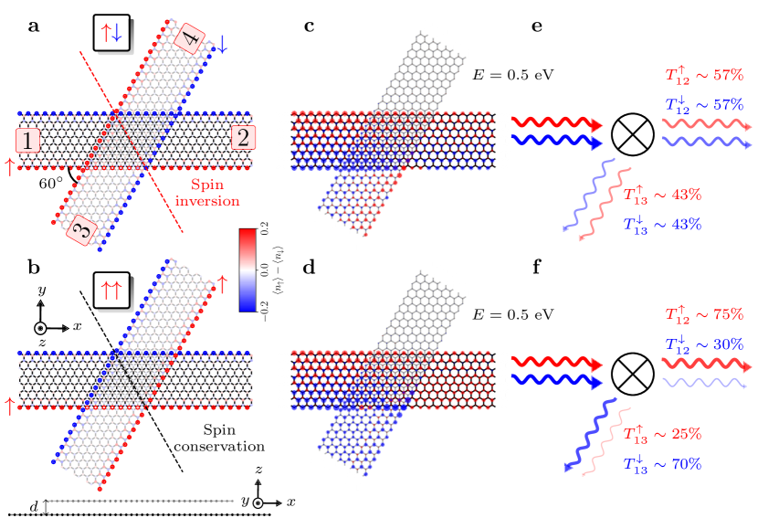
Figure 1(a) shows the device structure for two AB-stacked ZGNRs, each with a width of 8 carbon atoms (8-ZGNRs). In principle, away from the crossing (but within the spin correlation length), each of the four electrodes can be imposed one of the two possible symmetry-broken spin configurations at the edges, leading to unique boundary conditions for the device region. The self-consistent solutions to this problem are shown in Figs. S6 and S7 [41] for AB- and AA-stacked junctions, respectively, along with the electronic energy differences. The spin polarization for the two lowest-energy states with AB-stacking are shown in Fig. 1(a-b). In the following we label these as and , where the first (second) arrow refers to the spin orientation of the lower edge of the horizontal (inclined) GNR. Although the electronic energy of is found to be 82 meV above that of with AB-stacking, it is interesting to consider both configurations as this (constant) energy penalty may be compensated by a (length-dependent) energy preference for a certain polarization on the extended GNRs through interactions with their environment.
The spin- and energy-resolved transmission probability between any pair of electrodes can be computed from , where is the device Green’s function and the broadening matrix related to the self-energy from electrode and for spin-orientation [22, 39]. Similarly, the site-resolved density of scattering states can be computed as .
Figures 1(c-d) show the spatial distribution of the scattering states incoming from electrode 1 in the conduction band. At each lattice site the disk size is proportional to the density of states (summed over spin) while its color indicates the local majority spin. The electron energy is chosen at eV above the Fermi energy , i.e., slightly away from the window with edge states. This implies mode propagation involving only a single GNR subband, cf. Figs. S3 and S4 [41], as well as robustness against edge disorder [42]. Figures 1(c-d) also illustrate how the transmitted wave—for both spin configurations and —is split into electrodes 2 and 3 with negligible reflection and amplitude in electrode 4, as expected for the beam splitter. Conceptually, this is expressed with the representation in Fig. 1(e-f) along with the computed transmission probabilities.
Remarkably, and differ substantially when one considers the spin-resolved transmissions. Whereas does not polarize the current, since the transmission probabilities for both spin channels are equal, the configuration leads to a ratio , i.e., a spin filtering effect.
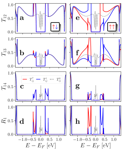
For further quantitative analysis, Fig. 2 reports the spin- and energy-resolved transmission and reflection probabilities for an electron injected from terminal into the (panels a-d) and (panels e-h) configurations. For comparison, each panel includes the corresponding results for the unpolarized device (, dashed gray lines) reported previously [29]. The introduction of Coulomb repulsion has two direct consequences: (i) it opens a transport gap near zero energy due to polarization of the edge bands, and (ii) it shifts the states at the Brillouin zone boundary (Figs. S3 and S4 [41]) resulting in the formation of two transverse modes at very low energy. While the beam splitting effect in the two-mode energy range is hampered by substantial scattering and reflection (Fig. 2d,h), it is completely restored in the energy range with only a single mode, i.e., 0.4 eV 1.3 eV, a condition already identified for unpolarized devices [29]. In fact, the transmission properties for coincides there with those of the unpolarized device (Fig. 2a-d). On the other hand, for the configuration the probabilities and show a strong spin splitting (Fig. 2e-h), revealing that the spin-filtering effect emphasized in Fig. 1(d,f) exists for the whole band.
This qualitative difference between and can be understood by considering the different symmetries that apply to these two configurations. Geometrically, the considered AB-stacked structure possesses one mirror-symmetry plane as shown by the dashed lines in Fig. 1(a,b) [29]. The difference emerges when one considers symmetry-lowering by the spin polarization: For the spin index maps into the opposite through the mirror operation (red axis) while for the spin index is conserved. More specifically for , these spatial symmetries impose constraints in the transmission probabilities between the spin channels, e.g., that , , etc. Further, considering probability conservation for injection from electrodes 1 or 2 one has the relations (valid when ). Together with time-reversal symmetry () it follows that in the case of , i.e., that the transmissions are spin independent. For no such condition applies and the spin channels are decoupled and the transmission probabilities may be very different. Indeed, this is directly seen in our calculations.
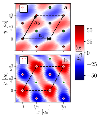
If we consider junction imperfections the aforementioned symmetry constraint would be absent and the spin-polarizing effect no longer symmetry forbidden. To examine the relationship between geometry and transport properties we use as a measure the spin polarization in the transmission between a pair of electrodes:
| (2) |
Figure 3 shows at eV as a function of in-plane translations of one ribbon with respect to the other for both and configurations. The AB- and AA-stacked geometries are indicated with symbols in the density plots. Evidently, away from these high-symmetry situations the spin-polarizing effect is generally present. The same conclusion holds true also for a range of twist angles (Sec. S11 [41]).
At this point it should be noted that it may be difficult to prepare the device in one specific spin configuration, such as the low-energy states and discussed up to now. For instance, it is not possible to tune which one is the energetically lower (and thus at low temperatures thermally stable) state by a homogeneous magnetic field as the Zeeman energy is the same for both solutions. On the other hand, transverse electric fields across the individual electrodes [8] or injection of spin-polarized currents at the edges from the tip of an STM [43] could potentially be strategies to control their magnetization. Nevertheless, our fundamental assumption is that the different collective spin states of the device are sufficiently long lived and robust to be probed by a transient current pulse. This assumption is supported by the fact that our calculations predict that the electronic energy is increased by about 0.20 eV when a magnetic domain wall is inserted into a 8-ZGNR (Figs. S6 and S7 [41]), an indication of a very large barrier even compared to room temperature.
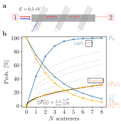
The spin-polarizing effect of a single junction discussed above can be enhanced by placing several consecutive crossings to form an array of scatterers as displayed in Fig. 4(a). Because back-scattering is negligible in the single-mode energy region, we can approximate the overall transmission probability across an array of crossings as where is the transmission of the th junction. This approximation was tested for the case of and shows an excellent agreement compared to a calculation of the full device (Sec. S9 [41]). This idea is exemplified in Fig. 4(b) for two different scenarios: an ideal arrangement of identical AB-stacked configurations (blue circles) as well as a more realistic situation corresponding to random sampling (orange squares, Sec. S12 [41]) over different spin-, intersection angle (within 55-65∘), and translation configurations. This shows that with four crossings the total current polarization can reach with a transmission of in the ideal case. Even in the pessimistic case with random junctions, where partial cancellation can occur due to sign changes in the individual , the spin polarization of the array approaches 1 exponentially in (black curve, see [41]). The best 1st percentile (top gray curve) of the sampled arrays still reaches for . Although this statistical analysis—described in detail in Sec. S12 [41]—is based on the simplifying assumption of equal weights of the configurations, it serves to illustrate that arrays can be interesting even if one does not have precise control over the individual junctions.
In conclusion, we have analyzed the spin-dependent transport properties of crossed ZGNRs using MFH and NEGF theory, and found that the beam-splitting effect reported previously survives in presence of Coulomb repulsions with two distinct modifications: a transport gap opens at low energies and a spin-dependent scattering potential emerges. Except for specific high-symmetry configurations, this class of electronic devices are generally predicted to behave as spin-polarizing beam splitters with interesting possibilities for electron quantum optics [44]. Such spin-dependent scattering potentials are also obtained with other edge-polarized nanoribbons (Sec. S13 [41]). By constructing arrays of junctions the spin-polarizing effect can be enhanced.
Although the proposed devices are ahead of current experiments, a rapid progress in bottom-up fabrication and scanning probe techniques makes it conceivable to assemble nearly defect-free junctions on insulating thin films [45], to drive coherent electron dynamics [46, 47], and to characterize electron transport by multi-probe setups [48] or through single-photon emission [49]. Our results add to the vision of using GNR-based devices for spintronics and quantum technologies. For instance, two spin-polarizing beam splitters in combination with a charge detector can be used to deterministically entangle a moving spin qubit [50]. Conversely, a spin-polarizing beam splitter can also be used to determine the entanglement of injected pairs of spins [51]. As an additional application, a high-fidelity spin filter allows ”spin-to-charge” conversion and thus a charge-measurement-based spin determination.
Acknowledgements.
This work was supported by the Spanish MCIN/AEI/ 10.13039/501100011033 (PID2020-115406GB-I00 and PID2019-107338RB-C66), the Basque Department of Education (PRE-2021-2-0190 and PIBA-2020-1-0014), the University of the Basque Country (IT1246-19), and the European Union (EU) through Horizon 2020 (FET-Open project “SPRING” Grant no. 863098).References
- Castro Neto et al. [2009] A. H. Castro Neto, F. Guinea, N. M. R. Peres, K. S. Novoselov, and A. K. Geim, “The electronic properties of graphene,” Rev. Mod. Phys. 81, 109 (2009).
- Yazyev [2010] O. V. Yazyev, “Emergence of magnetism in graphene materials and nanostructures,” Rep. Prog. Phys. 73, 056501 (2010).
- Han et al. [2014] W. Han, R. K. Kawakami, M. Gmitra, and J. Fabian, “Graphene spintronics,” Nat. Nanotechnol. 9, 794 (2014).
- González-Herrero et al. [2016] H. González-Herrero, J. M. Gómez-Rodríguez, P. Mallet, M. Moaied, J. J. Palacios, C. Salgado, M. M. Ugeda, J.-Y. Veuillen, F. Yndurain, and I. Brihuega, “Atomic-scale control of graphene magnetism by using hydrogen atoms,” Science 352, 437 (2016).
- Magda et al. [2014] G. Z. Magda, X. Jin, I. Hagymási, P. Vancsó, Z. Osváth, P. Nemes-Incze, C. Hwang, L. P. Biró, and L. Tapasztó, “Room-temperature magnetic order on zigzag edges of narrow graphene nanoribbons,” Nature 514, 608 EP (2014).
- Han and Kawakami [2011] W. Han and R. K. Kawakami, “Spin relaxation in single-layer and bilayer graphene,” Phys. Rev. Lett. 107, 047207 (2011).
- Tombros et al. [2007] N. Tombros, C. Jozsa, M. Popinciuc, H. T. Jonkman, and B. J. van Wees, “Electronic spin transport and spin precession in single graphene layers at room temperature,” Nature 448, 571 (2007).
- Son et al. [2006] Y.-W. Son, M. L. Cohen, and S. G. Louie, “Half-metallic graphene nanoribbons,” Nature 444, 347 (2006).
- Hancock et al. [2010] Y. Hancock, A. Uppstu, K. Saloriutta, A. Harju, and M. J. Puska, “Generalized tight-binding transport model for graphene nanoribbon-based systems,” Phys. Rev. B 81, 245402 (2010).
- Saffarzadeh and Farghadan [2011] A. Saffarzadeh and R. Farghadan, “A spin-filter device based on armchair graphene nanoribbons,” Appl. Phys. Lett. 98, 023106 (2011).
- Gregersen et al. [2017] S. S. Gregersen, S. R. Power, and A.-P. Jauho, “Nanostructured graphene for spintronics,” Phys. Rev. B 95, 121406 (2017).
- Trauzettel et al. [2007] B. Trauzettel, D. V. Bulaev, D. Loss, and G. Burkard, “Spin qubits in graphene quantum dots,” Nat. Phys. 3, 192 (2007).
- Pedersen et al. [2008] T. G. Pedersen, C. Flindt, J. Pedersen, N. A. Mortensen, A.-P. Jauho, and K. Pedersen, “Graphene antidot lattices: Designed defects and spin qubits,” Phys. Rev. Lett. 100, 136804 (2008).
- Jo et al. [2021] M. Jo, P. Brasseur, A. Assouline, G. Fleury, H.-S. Sim, K. Watanabe, T. Taniguchi, W. Dumnernpanich, P. Roche, D. C. Glattli, et al., “Quantum Hall valley splitters and a tunable Mach-Zehnder interferometer in graphene,” Phys. Rev. Lett. 126, 146803 (2021).
- Cai et al. [2010] J. Cai, P. Ruffieux, R. Jaafar, M. Bieri, T. Braun, S. Blankenburg, M. Muoth, A. P. Seitsonen, M. Saleh, X. Feng, et al., “Atomically precise bottom-up fabrication of graphene nanoribbons,” Nature 466, 470 (2010).
- Ruffieux et al. [2016] P. Ruffieux, S. Wang, B. Yang, C. Sánchez-Sánchez, J. Liu, T. Dienel, L. Talirz, P. Shinde, C. A. Pignedoli, D. Passerone, et al., “On-surface synthesis of graphene nanoribbons with zigzag edge topology,” Nature 531, 489 (2016).
- Koch et al. [2012] M. Koch, F. Ample, C. Joachim, and L. Grill, “Voltage-dependent conductance of a single graphene nanoribbon,” Nat. Nanotechnol. 7, 713 (2012).
- Kawai et al. [2016] S. Kawai, A. Benassi, E. Gnecco, H. Söde, R. Pawlak, X. Feng, K. Müllen, D. Passerone, C. A. Pignedoli, P. Ruffieux, et al., “Superlubricity of graphene nanoribbons on gold surfaces,” Science 351, 957 (2016).
- Jiao et al. [2010] L. Jiao, L. Zhang, L. Ding, J. Liu, and H. Dai, “Aligned graphene nanoribbons and crossbars from unzipped carbon nanotubes,” Nano Research 3, 387 (2010).
- Wortmann et al. [2001] D. Wortmann, S. Heinze, P. Kurz, G. Bihlmayer, and S. Blügel, “Resolving complex atomic-scale spin structures by spin-polarized scanning tunneling microscopy,” Phys. Rev. Lett. 86, 4132 (2001).
- Burtzlaff et al. [2015] A. Burtzlaff, A. Weismann, M. Brandbyge, and R. Berndt, “Shot noise as a probe of spin-polarized transport through single atoms,” Phys. Rev. Lett. 114, 016602 (2015).
- Büttiker et al. [1985] M. Büttiker, Y. Imry, R. Landauer, and S. Pinhas, “Generalized many-channel conductance formula with application to small rings,” Phys. Rev. B 31, 6207 (1985).
- Areshkin and White [2007] D. A. Areshkin and C. T. White, “Building blocks for integrated graphene circuits,” Nano Lett. 7, 3253 (2007).
- Jayasekera and Mintmire [2007] T. Jayasekera and J. W. Mintmire, “Transport in multiterminal graphene nanodevices,” Nanotechn. 18, 424033 (2007).
- Botello-Méndez et al. [2011] A. R. Botello-Méndez, E. Cruz-Silva, J. M. Romo-Herrera, F. López-Urías, M. Terrones, B. G. Sumpter, H. Terrones, J.-C. Charlier, and V. Meunier, “Quantum transport in graphene nanonetworks,” Nano Lett. 11, 3058 (2011).
- Cary et al. [2014] T. Cary, E. Costa Girão, and V. Meunier, “Electronic properties of three-terminal graphitic nanowiggles,” Phys. Rev. B 90, 115409 (2014).
- Lima et al. [2016] L. R. F. Lima, A. R. Hernández, F. A. Pinheiro, and C. Lewenkopf, “A 50/50 electronic beam splitter in graphene nanoribbons as a building block for electron optics,” J. Phys.: Condens. Matter 28, 505303 (2016).
- Brandimarte et al. [2017] P. Brandimarte, M. Engelund, N. Papior, A. Garcia-Lekue, T. Frederiksen, and D. Sánchez-Portal, “A tunable electronic beam splitter realized with crossed graphene nanoribbons,” J. Chem. Phys. 146, 092318 (2017).
- Sanz et al. [2020] S. Sanz, P. Brandimarte, G. Giedke, D. Sánchez-Portal, and T. Frederiksen, “Crossed graphene nanoribbons as beam splitters and mirrors for electron quantum optics,” Phys. Rev. B 102, 035436 (2020).
- Brey and Fertig [2006] L. Brey and H. A. Fertig, “Electronic states of graphene nanoribbons studied with the Dirac equation,” Phys. Rev. B 73, 235411 (2006).
- Wakabayashi et al. [2007] K. Wakabayashi, Y. Takane, and M. Sigrist, “Perfectly conducting channel and universality crossover in disordered graphene nanoribbons,” Phys. Rev. Lett. 99, 036601 (2007).
- Fujita et al. [1996] M. Fujita, K. Wakabayashi, K. Nakada, and K. Kusakabe, “Peculiar localized state at zigzag graphite edge,” J. Phys. Soc. Jpn. 65, 1920 (1996).
- Blackwell et al. [2021] R. E. Blackwell, F. Zhao, E. Brooks, J. Zhu, I. Piskun, S. Wang, A. Delgado, Y.-L. Lee, S. G. Louie, and F. R. Fischer, “Spin splitting of dopant edge state in magnetic zigzag graphene nanoribbons,” Nature 600, 647 (2021).
- Wimmer et al. [2008] M. Wimmer, I. Adagideli, S. Berber, D. Tománek, and K. Richter, “Spin currents in rough graphene nanoribbons: Universal fluctuations and spin injection,” Phys. Rev. Lett. 100, 177207 (2008).
- Sanz et al. [2021] S. Sanz, N. Papior, M. Brandbyge, and T. Frederiksen, “hubbard: v0.1.0,” (2021).
- Hubbard [1963] J. Hubbard, “Electron correlations in narrow energy bands,” Proc. R. Soc. A 276, 238 (1963).
- Fernández-Rossier and Palacios [2007] J. Fernández-Rossier and J. J. Palacios, “Magnetism in graphene nanoislands,” Phys. Rev. Lett. 99, 177204 (2007).
- Li et al. [2019] J. Li, S. Sanz, M. Corso, D. J. Choi, D. Peña, T. Frederiksen, and J. I. Pascual, “Single spin localization and manipulation in graphene open-shell nanostructures,” Nat. Commun. 10, 200 (2019).
- Papior et al. [2017] N. Papior, N. Lorente, T. Frederiksen, A. García, and M. Brandbyge, “Improvements on non-equilibrium and transport green function techniques: The next-generation TranSiesta,” Comp. Phys. Commun. 212, 8 (2017).
- Papior [2021] N. Papior, “sisl: v0.11.0,” (2021).
- [41] See Supplemental Material [url] for details on methodology and additional calculations, which includes Refs. [52-58].
- Zârbo and Nikolić [2007] L. P. Zârbo and B. K. Nikolić, “Spatial distribution of local currents of massless Dirac fermions in quantum transport through graphene nanoribbons,” Europhys. Lett. (EPL) 80, 47001 (2007).
- Loth et al. [2010] S. Loth, K. von Bergmann, M. Ternes, A. F. Otte, C. P. Lutz, and A. J. Heinrich, “Controlling the state of quantum spins with electric currents,” Nat. Phys. 6, 340 (2010).
- Bocquillon et al. [2014] E. Bocquillon, V. Freulon, F. D. Parmentier, J.-M. Berroir, B. Plaçais, C. Wahl, J. Rech, T. Jonckheere, T. Martin, C. Grenier, et al., “Electron quantum optics in ballistic chiral conductors,” Ann. Phys. 526, 1 (2014).
- Jacobse et al. [2018] P. Jacobse, M. J. J. Mangnus, S. J. M. Zevenhuizen, and I. Swart, “Mapping the conductance of electronically decoupled graphene nanoribbons,” ACS Nano 12, 7048 (2018).
- Baumann et al. [2015] S. Baumann, W. Paul, T. Choi, C. P. Lutz, A. Ardavan, and A. J. Heinrich, “Electron paramagnetic resonance of individual atoms on a surface,” Science 350, 417 (2015).
- Ammerman et al. [2021] S. E. Ammerman, V. Jelic, Y. Wei, V. N. Breslin, M. Hassan, N. Everett, S. Lee, Q. Sun, C. A. Pignedoli, P. Ruffieux, et al., “Lightwave-driven scanning tunnelling spectroscopy of atomically precise graphene nanoribbons,” Nat. Commun. 12, 6794 (2021).
- Kolmer et al. [2019] M. Kolmer, P. Brandimarte, J. Lis, R. Zuzak, S. Godlewski, H. Kawai, A. Garcia-Lekue, N. Lorente, T. Frederiksen, C. Joachim, et al., “Electronic transport in planar atomic-scale structures measured by two-probe scanning tunneling spectroscopy,” Nat. Commun. 10, 1573 (2019).
- Chong et al. [2018] M. C. Chong, N. Afshar-Imani, F. Scheurer, C. Cardoso, A. Ferretti, D. Prezzi, and G. Schull, “Bright electroluminescence from single graphene nanoribbon junctions,” Nano Lett. 18, 175 (2018).
- Beenakker et al. [2004] C. W. J. Beenakker, D. P. DiVincenzo, C. Emary, and M. Kindermann, “Charge detection enables free-electron quantum computation,” Phys. Rev. Lett. 93, 020501 (2004).
- Mazza et al. [2013] F. Mazza, B. Braunecker, P. Recher, and A. Levy Yeyati, “Spin filtering and entanglement detection due to spin-orbit interaction in carbon nanotube cross-junctions,” Phys. Rev. B 88, 195403 (2013).
- Feldner et al. [2011] H. Feldner, Z. Y. Meng, T. C. Lang, F. F. Assaad, S. Wessel, and A. Honecker, “Dynamical signatures of edge-state magnetism on graphene nanoribbons,” Phys. Rev. Lett. 106, 226401 (2011).
- Brandbyge et al. [2002] M. Brandbyge, J.-L. Mozos, P. Ordejón, J. Taylor, and K. Stokbro, “Density-functional method for nonequilibrium electron transport,” Phys. Rev. B 65, 165401 (2002).
- Sancho et al. [1985] M. P. L. Sancho, J. M. L. Sancho, J. M. L. Sancho, and J. Rubio, “Highly convergent schemes for the calculation of bulk and surface Green functions,” J. Phys. F: Met. Phys. 15, 851 (1985).
- Asano and Nakamura [2019] T. Asano and J. Nakamura, “Edge-state-induced stacking of zigzag graphene nanoribbons,” ACS Omega 4, 22035 (2019).
- Mostaani et al. [2015] E. Mostaani, N. D. Drummond, and V. I. Fal’ko, “Quantum Monte Carlo calculation of the binding energy of bilayer graphene,” Phys. Rev. Lett. 115, 115501 (2015).
- Lee et al. [2005] H. Lee, Y.-W. Son, N. Park, S. Han, and J. Yu, “Magnetic ordering at the edges of graphitic fragments: Magnetic tail interactions between the edge-localized states,” Phys. Rev. B 72, 174431 (2005).
- Cahay et al. [1988] M. Cahay, M. McLennan, and S. Datta, “Conductance of an array of elastic scatterers: A scattering-matrix approach,” Phys. Rev. B 37, 10125 (1988).
See pages ,- of supp-info.pdf