Light Sources with Bias Tunable Spectrum
based on van der Waals Interface Transistors
Abstract
Light-emitting electronic devices are ubiquitous in key areas of current technology, such as data communications, solid-state lighting, displays, and optical interconnects. Controlling the spectrum of the emitted light electrically, by simply acting on the device bias conditions, is an important goal with potential technological repercussions. However, identifying a material platform enabling broad electrical tuning of the spectrum of electroluminescent devices remains challenging. Here, we propose light-emitting field-effect transistors based on van der Waals interfaces of atomically thin semiconductors as a promising class of devices to achieve this goal. We demonstrate that large spectral changes in room-temperature electroluminescence can be controlled both at the device assembly stage –by suitably selecting the material forming the interfaces– and on-chip, by changing the bias to modify the device operation point. Even though the precise relation between device bias and kinetics of the radiative transitions remains to be understood, our experiments show that the physical mechanism responsible for light emission is robust, making these devices compatible with simple large areas device production methods.
Introduction
Since the discovery that monolayer semiconducting transition metal dichalcogenides (TMDs) are direct gap semiconductors exhibiting strong luminescence 1, 2, two-dimensional (2D) materials have attracted interest for optoelectronic applications 3, 4, 5, 6. Their potential stems from the ease with which the electronic properties of 2D semiconductors can be tuned by different means 7, 8, 9, 10, 11. In phosporene, for instance, mechanical strain can be used to tune the band gap by a very large amount, resulting in a controllable change of the wavelength of emitted light, as observed in recent photoluminescence measurements 12. In semiconducting TMDs, electrostatic gating gives access to a variety of excitonic states with different energy 13, 14, an effect that has been used to realize bias tunable electroluminescent devices with emission energy that has been varied by several tens of meV 9, 11. Realizing electroluminescent devices enabling much broader changes in the spectrum of the emitted light by simply acting on the device operation point (i.e., on the device bias) has however not been possible so far.
Light-emitting field-effect transistors (LEFETs) are three-terminal devices that allow switching of both the electrical conductance and light emission 15, 16, 17, 18, 19. They rely on semiconductors that support ambipolar transport to inject simultaneously in the transistor channel electrons and holes 20, whose radiative recombination is the origin of the emitted light 21, 22. Past research on LEFETs has concentrated on organic semiconductors, which have suitable properties for their realization 18, 19, 23, 24, 25. Ionic gated LEFETs based on 2D semiconductors are a recently discovered alternative that offer potential advantages, such as higher and well-balanced electron and hole mobilities, as well as low-bias operation 26, 27, 28, 29, 30. Efficient LEFETs, however, require the use of 2D semiconductors with a direct bandgap, whose paucity limits the possibility to tune the spectrum of the emitted light. Van der Waals (vdW) interfaces formed by atomically thin semiconducting materials provide a strategy to address this issue because the wavelength of light emitted by interlayer transitions (electrons hosted in one layer recombining with holes hosted in the other) can be engineered by selecting constituent materials with an appropriate band
alignment 31, 32, 33, 34, 35.
Here, we demonstrate experimentally LEFETs realized on vdW interfaces, and show that they can be operated as electrically tunable light sources. As compared to LEFETs based on individual monolayers, devices fabricated on vdW interfaces potentially offer more functionality. The electronic structure of the individual layers, for instance, is often only minorly affected by the interface formation, so that a rich set of electronic levels –i.e., the bands of the two materials, including the sub-bands originating from quantum confinement– is present 36, 37, 38, 39, 40. If properly populated by acting on the device operation point (i.e., the applied source-drain and gate voltages, and , respectively), these levels may enable the energy of the emitted light to be tuned. Additionally, the electric field perpendicular to the transistor channel creates a potential difference between the layers forming the interface, which shifts the energy of the recombining electrons and holes 41, 42. The wavelength of light generated by interlayer transitions is expected to shift accordingly, providing another route to tune the emission spectrum by acting on the device operation point. These ideas disclose possible mechanisms to operate LEFETs based on vdW interfaces as electrically tunable light sources. However, neither their validity nor the potential of LEFETs based on vdW interfaces has been assessed so far.
Here, we show that light-emitting transistors based on a recently discovered type of van der Waals (vdW) heterostructures –which we refer to as - interfaces (see discussion below)– exhibit room-temperature electroluminescence that can be tuned over a much broader spectral range (from below 1.2 to 1.7 eV, in the devices reported here) by acting exclusively on the device operation point. Our work relies on devices made of bilayers (2L) of semiconducting transition metal dichalcogenides (TMDs; we use WS2 and MoS2) and InSe multilayers , to form vdW interfaces that belong to a recently identified class exhibiting robust radiative interlayer transitions (e.g., transitions that are radiative irrespective of the lattice structure of the constituent materials or of their relative orientation) 38, 43, 44. The robustness originates from having the conduction and valence band extrema in the two layers at = 0, i.e., at the -point of the Brillouin zone ( which is why we refer to these systems as to - interfaces. It is important because it facilitates the device assembly, and makes it compatible with simple large-area production techniques 9, 45. Indeed, we find that all our LEFETs exhibit electroluminescence, with a wavelength that can be engineered by selecting the constituent layers, and with a spectrum that can be tuned by acting on the device operation point. Contrary to earlier studies of - interfaces 44 –in which photoluminescence (PL) was only observed at cryogenic temperatures– electroluminescence (EL) is already present at room temperature, a key finding when assessing the technological potential of these devices.
Results
Device fabrication and characterization
Ionic gated LEFETs (see Figure 1a-c and Supplementary Section 1) based on 2L-TMD/InSe vdW interfaces (see Figure 1d) are realized using techniques commonly employed for the assembly of structures based on 2D materials 46. TMD bilayers and InSe multilayers are exfoliated from bulk crystals onto Si/SiO2 substrates. Heterostructures are formed by picking up layers one after the other, and transferring the resulting interface onto a fresh Si/SiO2 substrate, with the TMD layer covering the InSe one and effectively encapsulating it (which is important in view of the non-perfect stability of InSe in ambient; the interface assembly process is carried out in the controlled atmosphere of a glove box). Source and drain contacts, as well as a large pad acting as gate electrode, are defined by means of electron beam lithography, electron-beam evaporation of a Pt-Au film (5/30 nm) and lift off (see Figure 1e). Subsequently, a window in PMMA is patterned to define the region where the ionic liquid ((N,N-diethyl-N-methyl-N-(2-methoxyethyl) ammonium bis(trifluoromethylsulfonyl) imide) commonly referred to as DEME-TFSI) contacts the interface. The liquid is applied as a final step, prior to inserting the devices in a vacuum chamber with optical access (see Methods section for more details).
The WS2 and MoS2 crystals used for exfoliation are purchased from HQ Graphene. InSe is a less commonly employed compound and care is needed because the crystal quality varies strongly depending on details of the growth process. Lower quality can result in a large density of defects 47, 48, 49 that create in-gap states acting as hole traps, which is why our earlier attempts to use InSe crystals to realize vdW interface LEFETs failed (in-gap states prevent the electrostatic accumulation of holes in the valence band of the TMD, and impede ambipolar transport). The InSe crystals that we employ here, grown at Florida State University (see Methods Section for details of the growth process), appear to have high quality and a low density of defects, as we directly infer from the transistor electrical characteristics and from the narrow lines observed in PL studies of h-BN-encapsulated multilayers (see Figure 1f).
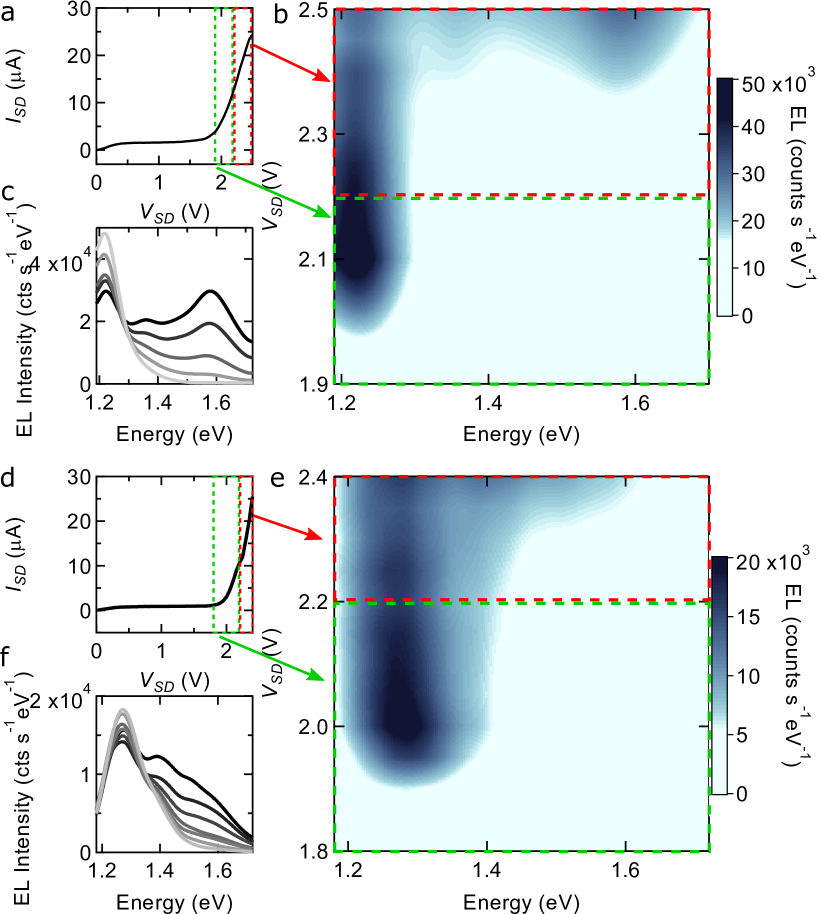
Figure 2a shows the room-temperature transfer curve (source-drain current versus gate voltage at fixed source-drain voltage = 50 mV) of a device realized on a 2L-WS2/4L-InSe interface. The behavior is typical of ambipolar transistors with current mediated by holes and electrons flowing for sufficiently large negative and positive , respectively 50, 51, 52, 26, 24, 53, 54, 55. Accumulation of electrons and holes leads to comparable current levels, confirming that transport is well-balanced and that residual defects in InSe do not prevent high-quality device operation. When plotted in logarithmic scale (Figure 2b) the data allow determining the subthreshold swing , equal to = 115 and 90 mV/decade near the threshold for hole and electron conduction, respectively (other devices exhibit values even closer to the ultimate room-temperature limit of 60 mV/decade) 56. The output curves (-vs- plotted for different, fixed ) shown in Figure 2c and 2d also exhibit the expected behavior. Upon increasing , increases linearly at first then saturates, and eventually exhibits a very steep increase, when entering the ambipolar injection regime. This regime –in which electrons and holes are injected at opposite contacts– is the one of interest for LEFET operation (see Supplementary Section 1), and can be reached irrespective of the polarity of the applied gate voltage.
Electroluminescence from vdW interface LEFET
EL is expected to occur concomitantly with ambipolar injection, with light emission starting at one of the contacts and shifting into the channel as is further increased.18 This is indeed what we observe (see Figure 3a as well as Supplementary Figure 2 and accompanying discussion in Supplementary Section 1). The light emitted by the LEFET is collected by a microscope objective and fed into a spectrometer. The spectral analysis performed on data measured at fixed , by increasing past the onset of the ambipolar injection regime ( > +1.9 V in Figure 3b for > 0 and < -2.2 V in Figure 3e for < 0 V), is shown in Figures 3c and 3d for > 0 V, and in Figures 3f and 3g for < 0 V. As the current increases exponentially rapidly, we initially limit the maximum applied to avoid damaging the devices. EL is detected in all cases, with an intensity that increases rapidly with . The light exhibits a dominant spectral line just above 1.2 eV, irrespective of the precise value of and of whether has positive or negative polarity (an additional shoulder at 1.4 eV is visible for < 0, see Figure 3g, is also present –albeit less pronounced– for > 0).
In Figure 3h, we plot the device EL spectrum (red line; = +0.5 V and = +2.2 V) together with the PL spectrum of 4L-InSe (purple line; PL is measured at = 5 K, since no signal is observed at room temperature) and 2L-WS2 (blue line). The energy of the EL peak is considerably lower than the recombination energy in either 4L-InSe or 2L-WS2, as expected for an interlayer transition 44. The energy of the room-temperature EL signal (Figure 3j, thick line) matches that of low-temperature interlayer transitions seen in PL (Figure 3j, thin line) due to electrons in InSe recombining with holes in WS2, if we take into account that the TMD and the InSe gap typically increases by approximatively 50-100 meV upon cooling from 300 to 5 K 57, 14, 58, 59. The measurements, therefore, confirm that our LEFET operates as anticipated, with electrons injected in the InSe layer and holes in the WS2 one recombining via an interlayer transition. Finding that this transition results in EL even at room temperature is a positive, unexpected surprise.
Devices based on other - vdW interfaces should exhibit all key properties of 2L-WS2/4L-InSe LEFETs. We verify that this is indeed the case using transistors realized on interfaces of 2L-MoS2 (instead of 2L-WS2), and 3L-, 4L-, and 5L-InSe. Without going through all details (see Supplementary Section 2), the data show the occurrence of ambipolar transport (Figure 4a) and of the ambipolar injection regime past saturation (Figure 4b). Upon entering the ambipolar injection regime, EL is observed resulting in a line at 1.3 eV (for 2L-MoS2/5L-InSe) independently of (see Figure 4c and 4d), i.e., an energy lower than that of the transitions in the constituent materials (see Figure 4e). Figure 4f overviews the results obtained, by plotting together the room-temperature EL spectrum of LEFETs fabricated on all different vdW interfaces, and shows that combining different 2D materials indeed allows a dense coverage of part of the near-infrared and visible spectral range. Selecting multilayers of different thicknesses or having different compositions (e.g., MoSe2 or MoTe2) would further broaden the accessible spectrum, both on the higher and lower end 38, 43, 44.
Electrically tunable EL spectrum in vdW interface LEFET
Having established that LEFETs based on - interfaces provide a robust platform to generate room-temperature EL, we test whether the light spectrum can be controlled by varying the device operation point. Figure 5 illustrates the evolution of the spectrum of the light emitted by a 2L-WS2/4L-InSe (Figure 5a-c) and by a 2L-MoS2/5L-InSe (Figure 5d-f) LEFETs, upon pushing the source-drain bias to reach deeper in the ambipolar transport regime. The green rectangle in Figure 5a delimits the interval discussed earlier, and the corresponding part of the spectrum in Figure 5c (also delimited by a green rectangle) shows emission from the interlayer transition just above 1.2 eV, in agreement with the data shown in Figure 3b and 3c. When larger is applied, corresponding to the interval in the rectangle delimited by the red line in Figure 5a, the spectrum evolves. Additional transitions appear, visible in Figure 5b in the region delimited by the red rectangle, as well as in Figure 5c, which shows the spectrum of the emitted light at specific values of . A qualitatively identical behavior is observed in LEFETs based on 2L-MoS2/5L-InSe, with the regime of lower and higher highlighted by red and green rectangles in Figure 5d and the corresponding spectra shown in Figure 5e and 5f.
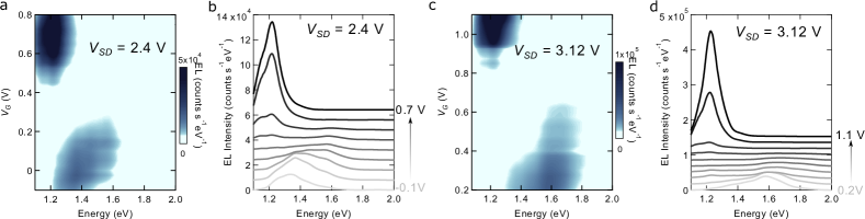
We have also measured the spectrum of the emitted light at a fixed value, as a function of , and found that in that case as well, the spectrum depends strongly on the device operation point. Figures 6a-d show the spectrum of the light emitted by a device realized on a 2L-WS2/4L-InSe interface, as a function of gate voltage, for two different values of source-drain bias ( = +2.4 V a-b and = +3.12 V c-d). Changing the gate voltage at fixed allows switching the spectrum of the light between two transitions visible in Figures 6b,c. In particular, at large positive gate voltage ( > +0.4 V in Figure 6a and > +0.8 V in Figure 6c), the spectrum of the emitted light is dominated by the interlayer transition at 1.2 eV between the bottom of the InSe conduction band and the top of the TMD valence band. At low gate voltage ( < +0.2 V in Figure 6a and < +0.6 V in Figure 6c), instead, light is emitted by another transition (possibly by multiple transitions, as suggested by the broad linewidth) at higher energy (approximately 1.4 eV), which appears to blue shift upon increasing . Unexpectedly, the two regimes are separated by an interval of gate voltages in which the power of emitted light vanishes (or is below the sensitivity of our detector). Finding that the gate allows switching the spectrum between two different emission lines is interesting, as it may provide new functionality to these LEFETs devices.
As part of our experiments, we have also determined the external quantum efficiency of our devices –i.e., the ratio between the number of emitted photons detected in our set-up and the number of injected electrons– by comparing the measured EL signal to the signal measured (with the same set-up) when using a commercial light-emitting diode as source. We found that, in the experimental configuration employed to detect EL, the external quantum efficiency of our devices is approximately 0.005 %, three orders of magnitude smaller than that of commercial devices. It should be realized, however, that in our set-up the external quantum efficiency is much lower than the actual quantum efficiency, because the optical selection rules for interlayer transitions 37, 60 dictate that light is mostly emitted in the plane of the interface. This implies that the majority of the photons emitted by our light-emitting transistors are not collected by the microscope objective, and that adopting strategies to improve the light outcoupling should lead to a drastic enhancement of the measured external quantum efficiency.
Irrespective of these considerations about the external quantum efficiency, our observation that the EL spectrum does depend on the device operation point proves that LEFETs based on vdW interfaces are indeed electrically tunable light sources. Understanding in detail how the EL spectrum depends on the LEFET operation point is however complex, both because different processes likely play a role, and because screening due to charges accumulated in the transistor channel can strongly (and non-linearly) affect the potential difference between the two layers forming the interface, especially in the region of the transistor channel where electron-hole recombination occurs. At sufficiently large , we expect that electrons are injected not only in the conduction band of InSe but also in that of the TMD, so that light can be emitted also from intralayer transitions within the TMD. This may account for the peak centered around 1.6 eV in 2L-WS2/4L-InSe, which corresponds well to one of the 2L-WS2 PL peaks. An intralayer transition in the semiconducting TMD is likely also responsible for part of the broad peak around 1.5 eV in the MoS2-based interfaces (the energy matches one of the peaks observed in PL of 2L-MoS2). The less pronounced peaks near 1.4 eV (at comparable but different energies in the 2L-WS2 and the 2L-MoS2 devices; see Figure 5b and 5e) occur at an energy that changes slightly upon changing . As the energy of these peaks is lower than all known intralayer transitions in the respective systems, we attribute their origin to an interlayer transition between an electron in a higher energy InSe sub-band recombining with a hole in the TMD (whose precise energy is affected by the electrostatic potential difference between the layers). This attribution is also consistent with data taken at fixed upon varying (see Figure 6), in which the transition energy is seen to blue shift upon changing the gate voltage.
More work is clearly needed to understand in detail the electroluminescence spectrum of - interfaces at large biases, as well as its evolution with both source-drain and gate biases (as mentioned earlier, screening plays a major and complex role in the way spectral features shift as function of biases, and a quantitative description will require a separate, dedicated modeling effort). We note, however, that the spectrum of light emitted by LEFETs based on monolayer TMDs remains unchanged even under driving the device with very large source-drain biases, as discussed in Supplementary Section 3 and shown in Figure S4 in there. The data, therefore, appear to substantiate our initial idea –namely that LEFETs based on vdW interfaces offer more functionalities than similar devices realized from individual monolayers– irrespective of the precise microscopic origin of the emitted light (i.e., of the specific transitions involved in the light emission process).
Discussion
The results presented above demonstrate the operation of vdW interface LEFETs and show that these transistors do allow the realization of light sources with a bias tunable spectrum. Finding that devices realized with multiple semiconducting TMDs and with InSe layers of different thickness lead to a qualitatively similar evolution of the spectrum of the emitted light with bias indicates that the operation mechanism is robust and of general validity. This robustness is important because –whereas only a few examples of electroluminescent devices with an electrically controllable spectrum have been reported in the past 61, 62, 63, 64– a large variety of 2D semiconductors exists that can be employed to realize light-emitting - interfaces.
It is clear that at this stage light-emitting transistors based on - vdW interfaces remain proof-of-principle devices and that considerable research is needed to characterize them and optimize their operation. We anticipate, for instance, that ionic liquid gating can be replaced by conventional solid-state gates using nm-thick h-BN dielectrics to separate the gate electrode from the vdW heterostructure. Indeed, h-BN layers that are a few nanometers thick exhibit breakdown field values approaching 1 V/nm 65, which are likely sufficient to achieve ambipolar transport and to operate the devices with larger than . Similarly –as already mentioned– the external quantum efficiency of our devices will need to be improved by adopting suitable strategies to optimize light outcoupling. While it is clear that at this stage different aspects of the device require improvements, it is worth re-iterating that - interfaces used within a light-emitting transistor configuration represent a platform that offers a very high potential for the realization of electroluminescent devices with bias tunable spectrum, and that satisfies many key requirements essential to the development of a successful technology. These include room-temperature operation and insensitivity of the devices to details of their assembly process, which ensures their robust operation. It is for these reasons that exploring the development of light-emitting transistors based on - interfaces appears to be promising for future device applications.
Methods
Crystal growth
InSe single crystals were grown through the Bridgman method: 6N-pure indium and 5N-pure selenium pellets in an atomic ratio of 52:48 were sealed in an evacuated quartz ampule and subsequently placed into a radio frequency (RF) furnace where the RF power was gradually increased to raise the temperature up to 800 ° C. The ampule was then pulled through the hottest zone at a rate of 2 mm/hour. Single crystals were characterized via electron dispersive spectroscopy and aberration-corrected transmission electron microscopy. X-ray diffraction measurements confirmed that -InSe adopts the R3 space group (160) with unit cell dimensions = 4.08(2) Å and = 24.938(24) Å. The quality of the crystals grown in this way is illustrated by the different measurements presented in the main text, including the narrow photoluminescence spectrum measured on exfoliated multilayers encapsulated in between hBN crystals, and the ambipolar transport properties of InSe/TMD heterostructures.
Sample fabrication
The fabrication of the heterostructures used to perform the measurements discussed in the main text relies on conventional techniques that are commonly employed to manipulate atomically thin crystals46 and is briefly outlined here for completeness. Atomically thin layers of TMDs and InSe are obtained by mechanical exfoliation of bulk crystals in a nitrogen gas-filled glove box with a < 0.5 ppm concentration of oxygen and water. The exfoliated crystals are transferred onto Si/SiO2 substrates and suitable layers are identified by looking at their optical contrast under an optical microscope. The heterostructures are then assembled in the same glove box with by-now conventional pick-up and release techniques based on either PPC/PDMS (Poly(propylene carbonate) /polydimethylsiloxane) or PC/PDMS (polycarbonate) polymer stacks placed on glass slides 46. To avoid degradation of air-sensitive InSe crystals, the structures are assembled so that the InSe layer lays on a thick hBN layer ( 20 nm) and is covered by the TMD layer (thereby ensuring that the InSe layer is properly encapsulated in between air-stable materials). Metallic electrodes (Pt/Au) are attached to the TMD layer by conventional nanofabrication techniques using electron-beam lithography, electron-beam evaporation, and lift-off. The sample is wire-bonded with indium or gold wires to a chip carrier and a small amount of ionic liquid ((N,N-diethyl-N-methyl-N-(2-methoxyethyl) ammonium bis(trifluoromethylsulfonyl) imide) commonly referred to as DEME-TFSI) is dropcasted onto the surface of the substrate to cover the metallic gate electrode and the transistor channel. The device is then rapidly transferred into the vacuum chamber with optical access and pumped overnight to remove moisture from the ionic liquid prior to the optical and electrical investigations.
Optical measurements
The sample is mounted in a vacuum chamber positioned under an optical microscope, providing optical and electrical access to the sample. The photoluminescence and electroluminescence of our light-emitting field-effect transistors are collected with help of a microscope objective and sent to a Czerny-Turner monochromator with a grating of 150 grooves/mm (Andor Shamrock 500i). The signal is detected with a Silicon Charge Coupled Device (CCD) array (Andor Newton 970 EMCCD). For photoluminescence measurements, the sample is illuminated with a laser beam generated by a supercontinuum white light laser source combined with a contrast filter, allowing to set the illumination wavelength to 610 nm. The laser power is kept at 50 W, to avoid damaging the structures.
Transport measurements
The electrical characterization of our FET is performed in the same chamber used for optical measurements. The gate bias voltage is applied using either a Keithley 2400 source unit or a homemade low-noise voltage source. The current and voltage signals are amplified with homemade low-noise amplifiers, and the amplified signals are recorded with an Agilent 34410A digital multimeter unit.
Data availability
The data supporting the findings of this study are available free of charges from the Yareta repository of the University of Geneva. https://doi.org/10.26037/yareta:mze42hgmc5cqtdsqmeszkprfxm
References
- [1] Splendiani, A. et al. Emerging Photoluminescence in Monolayer MoS2. Nano Letters 10, 1271–1275 (2010). URL http://dx.doi.org/10.1021/nl903868w.
- [2] Mak, K. F., Lee, C., Hone, J., Shan, J. & Heinz, T. F. Atomically Thin MoS_{2}: A New Direct-Gap Semiconductor. Physical Review Letters 105, 136805 (2010). URL http://link.aps.org/doi/10.1103/PhysRevLett.105.136805.
- [3] Mak, K. F. & Shan, J. Photonics and optoelectronics of 2D semiconductor transition metal dichalcogenides. Nature Photonics 10, 216–226 (2016). URL https://www.nature.com/articles/nphoton.2015.282. Number: 4 Publisher: Nature Publishing Group.
- [4] Avouris, P., Heinz, T. F. & Low, T. (eds.) 2D Materials: Properties and Devices (Cambridge University Press, Cambridge, 2017). URL https://www.cambridge.org/core/books/2d-materials/A87B3521C3A8A5885319F58E6F387830.
- [5] Mueller, T. & Malic, E. Exciton physics and device application of two-dimensional transition metal dichalcogenide semiconductors. npj 2D Materials and Applications 2, 1–12 (2018). URL https://www.nature.com/articles/s41699-018-0074-2.
- [6] Shree, S., Paradisanos, I., Marie, X., Robert, C. & Urbaszek, B. Guide to optical spectroscopy of layered semiconductors. Nature Reviews Physics 3, 39–54 (2021). URL https://www.nature.com/articles/s42254-020-00259-1.
- [7] He, K., Poole, C., Mak, K. F. & Shan, J. Experimental Demonstration of Continuous Electronic Structure Tuning via Strain in Atomically Thin MoS2. Nano Letters 13, 2931–2936 (2013). URL https://doi.org/10.1021/nl4013166. Publisher: American Chemical Society.
- [8] Island, J. O. et al. Precise and reversible band gap tuning in single-layer MoSe2 by uniaxial strain. Nanoscale 8, 2589–2593 (2016). URL https://pubs.rsc.org/en/content/articlelanding/2016/nr/c5nr08219f. Publisher: The Royal Society of Chemistry.
- [9] Withers, F. et al. Heterostructures Produced from Nanosheet-Based Inks. Nano Letters 14, 3987–3992 (2014). URL https://doi.org/10.1021/nl501355j.
- [10] Withers, F. et al. Light-emitting diodes by band-structure engineering in van der Waals heterostructures. Nature Materials 14, 301–306 (2015). URL http://www.nature.com/articles/nmat4205.
- [11] Paur, M. et al. Electroluminescence from multi-particle exciton complexes in transition metal dichalcogenide semiconductors. Nature Communications 10, 1709 (2019). URL https://www.nature.com/articles/s41467-019-09781-y/. Number: 1 Publisher: Nature Publishing Group.
- [12] Kim, H. et al. Actively variable-spectrum optoelectronics with black phosphorus. Nature 596, 232–237 (2021). URL https://www.nature.com/articles/s41586-021-03701-1.
- [13] Mak, K. F. et al. Tightly bound trions in monolayer MoS2. Nature Materials 12, 207–211 (2013). URL http://www.nature.com/nmat/journal/v12/n3/abs/nmat3505.html.
- [14] Ross, J. S. et al. Electrical control of neutral and charged excitons in a monolayer semiconductor. Nature Communications 4, 1474 (2013). URL https://www.nature.com/articles/ncomms2498.
- [15] Feng, M., Holonyak, N. & Hafez, W. Light-emitting transistor: Light emission from InGaP/GaAs heterojunction bipolar transistors. Applied Physics Letters 84, 151–153 (2004). URL https://aip.scitation.org/doi/10.1063/1.1637950.
- [16] Hepp, A. et al. Light-Emitting Field-Effect Transistor Based on a Tetracene Thin Film. Physical Review Letters 91, 157406 (2003). URL https://link.aps.org/doi/10.1103/PhysRevLett.91.157406.
- [17] Rost, C. et al. Ambipolar light-emitting organic field-effect transistor. Applied Physics Letters 85, 1613–1615 (2004). URL https://aip.scitation.org/doi/10.1063/1.1785290.
- [18] Zaumseil, J., Friend, R. H. & Sirringhaus, H. Spatial control of the recombination zone in an ambipolar light-emitting organic transistor. Nature Materials 5, 69–74 (2006). URL https://www.nature.com/articles/nmat1537.
- [19] Takenobu, T. et al. High Current Density in Light-Emitting Transistors of Organic Single Crystals. Physical Review Letters 100, 066601 (2008). URL https://link.aps.org/doi/10.1103/PhysRevLett.100.066601.
- [20] Kang, M. S. & Frisbie, C. D. A Pedagogical Perspective on Ambipolar FETs. ChemPhysChem 14, 1547–1552 (2013). URL https://onlinelibrary.wiley.com/doi/abs/10.1002/cphc.201300014.
- [21] Meijer, E. J. et al. Solution-processed ambipolar organic field-effect transistors and inverters. Nature Materials 2, 678–682 (2003). URL https://www.nature.com/articles/nmat978.
- [22] Muccini, M. A bright future for organic field-effect transistors. Nature Materials 5, 605–613 (2006). URL https://www.nature.com/articles/nmat1699.
- [23] Capelli, R. et al. Organic light-emitting transistors with an efficiency that outperforms the equivalent light-emitting diodes. Nature Materials 9, 496–503 (2010). URL https://www.nature.com/articles/nmat2751.
- [24] Bisri, S. Z., Shimizu, S., Nakano, M. & Iwasa, Y. Endeavor of Iontronics: From Fundamentals to Applications of Ion-Controlled Electronics. Advanced Materials 29, 1607054 (2017). URL https://www.onlinelibrary.wiley.com/doi/abs/10.1002/adma.201607054.
- [25] Qin, Z., Gao, H., Dong, H. & Hu, W. Organic Light-Emitting Transistors Entering a New Development Stage. Advanced Materials 33, 2007149 (2021). URL https://onlinelibrary.wiley.com/doi/abs/10.1002/adma.202007149.
- [26] Jo, S., Ubrig, N., Berger, H., Kuzmenko, A. B. & Morpurgo, A. F. Mono- and Bilayer WS2 Light-Emitting Transistors. Nano Letters 14, 2019–2025 (2014).
- [27] Zhang, Y. J., Oka, T., Suzuki, R., Ye, J. T. & Iwasa, Y. Electrically Switchable Chiral Light-Emitting Transistor. Science 344, 725–728 (2014). URL https://www.science.org/doi/10.1126/science.1251329.
- [28] Lezama, I. G. et al. Surface transport and band gap structure of exfoliated 2H-MoTe 2 crystals. 2D Materials 1, 021002 (2014). URL https://doi.org/10.1088%2F2053-1583%2F1%2F2%2F021002.
- [29] Gutierrez-Lezama, I., Reddy, B. A., Ubrig, N. & Morpurgo, A. F. Electroluminescence from indirect band gap semiconductor ReS2. 2D Materials 3, 045016 (2016). URL http://stacks.iop.org/2053-1583/3/i=4/a=045016.
- [30] Ponomarev, E., Gutierrez-Lezama, I., Ubrig, N. & Morpurgo, A. F. Ambipolar Light-Emitting Transistors on Chemical Vapor Deposited Monolayer MoS2. Nano Letters 15, 8289–8294 (2015). URL http://dx.doi.org/10.1021/acs.nanolett.5b03885.
- [31] Ceballos, F., Bellus, M. Z., Chiu, H.-Y. & Zhao, H. Ultrafast Charge Separation and Indirect Exciton Formation in a MoS2-MoSe2 van der Waals Heterostructure. ACS Nano 8, 12717–12724 (2014). URL https://doi.org/10.1021/nn505736z.
- [32] Rivera, P. et al. Observation of long-lived interlayer excitons in monolayer MoSe2-WSe2 heterostructures. Nat. Commun. 6, 6242 (2015). URL http://www.nature.com/doifinder/10.1038/ncomms7242.
- [33] Lien, D.-H. et al. Large-area and bright pulsed electroluminescence in monolayer semiconductors. Nature Communications 9, 1229 (2018). URL https://www.nature.com/articles/s41467-018-03218-8/.
- [34] Wang, J., Verzhbitskiy, I. & Eda, G. Electroluminescent Devices Based on 2D Semiconducting Transition Metal Dichalcogenides. Advanced Materials 30, 1802687 (2018). URL https://onlinelibrary.wiley.com/doi/abs/10.1002/adma.201802687.
- [35] Ponomarev, E., Ubrig, N., Gutierrez-Lezama, I., Berger, H. & Morpurgo, A. F. Semiconducting van der Waals Interfaces as Artificial Semiconductors. Nano Letters 18, 5146–5152 (2018).
- [36] Amin, B., Singh, N. & Schwingenschlogl, U. Heterostructures of transition metal dichalcogenides. Physical Review B 92, 075439 (2015). URL http://link.aps.org/doi/10.1103/PhysRevB.92.075439.
- [37] Magorrian, S. J., Zolyomi, V. & Fal’ko, V. I. Electronic and optical properties of two-dimensional InSe from a DFT-parametrized tight-binding model. Physical Review B 94, 245431 (2016). URL https://link.aps.org/doi/10.1103/PhysRevB.94.245431.
- [38] Ozcelik, V. O., Azadani, J. G., Yang, C., Koester, S. J. & Low, T. Band alignment of two-dimensional semiconductors for designing heterostructures with momentum space matching. Physical Review B 94, 035125 (2016). URL https://link.aps.org/doi/10.1103/PhysRevB.94.035125.
- [39] Wilson, N. R. et al. Determination of band offsets, hybridization, and exciton binding in 2D semiconductor heterostructures. Science Advances 3, e1601832 (2017). URL https://www.science.org/doi/10.1126/sciadv.1601832.
- [40] Hamer, M. J. et al. Indirect to Direct Gap Crossover in Two-Dimensional InSe Revealed by Angle-Resolved Photoemission Spectroscopy. ACS Nano 13, 2136–2142 (2019). URL https://doi.org/10.1021/acsnano.8b08726.
- [41] Ciarrocchi, A. et al. Polarization switching and electrical control of interlayer excitons in two-dimensional van der Waals heterostructures. Nature Photonics 13, 131–136 (2019). URL https://www.nature.com/articles/s41566-018-0325-y.
- [42] Jauregui, L. A. et al. Electrical control of interlayer exciton dynamics in atomically thin heterostructures. Science 366, 870–875 (2019). URL https://www.science.org/doi/10.1126/science.aaw4194.
- [43] Terry, D. J. et al. Infrared-to-violet tunable optical activity in atomic films of GaSe, InSe, and their heterostructures. 2D Materials 5, 041009 (2018). URL http://stacks.iop.org/2053-1583/5/i=4/a=041009.
- [44] Ubrig, N. et al. Design of van der Waals interfaces for broad-spectrum optoelectronics. Nature Materials 19, 299–304 (2020).
- [45] Hu, G. et al. Functional inks and printing of two-dimensional materials. Chemical Society Reviews 47, 3265–3300 (2018). URL https://pubs.rsc.org/en/content/articlelanding/2018/cs/c8cs00084k.
- [46] Zomer, P. J., Dash, S. P., Tombros, N. & van Wees, B. J. A transfer technique for high mobility graphene devices on commercially available hexagonal boron nitride. Appl. Phys. Lett. 99, 232104 (2011). URL https://aip.scitation.org/doi/abs/10.1063/1.3665405.
- [47] Chevy, A. Improvement of growth parameters for Bridgman-grown InSe crystals. Journal of Crystal Growth 67, 119–124 (1984). URL https://linkinghub.elsevier.com/retrieve/pii/0022024884901404.
- [48] Kudrynskyi, Z. et al. Giant Quantum Hall Plateau in Graphene Coupled to an InSe van der Waals Crystal. Physical Review Letters 119, 157701 (2017). URL https://link.aps.org/doi/10.1103/PhysRevLett.119.157701.
- [49] Arora, H. et al. Effective Hexagonal Boron Nitride Passivation of Few-Layered InSe and GaSe to Enhance Their Electronic and Optical Properties. ACS Applied Materials & Interfaces 11, 43480–43487 (2019). URL https://doi.org/10.1021/acsami.9b13442.
- [50] Podzorov, V., Gershenson, M. E., Kloc, C., Zeis, R. & Bucher, E. High-mobility field-effect transistors based on transition metal dichalcogenides. Applied Physics Letters 84, 3301 (2004). URL http://apl.aip.org/resource/1/applab/v84/i17/p3301_s1.
- [51] Zhang, Y., Ye, J., Matsuhashi, Y. & Iwasa, Y. Ambipolar MoS2 Thin Flake Transistors. Nano Letters 12, 1136–1140 (2012). URL http://dx.doi.org/10.1021/nl2021575.
- [52] Braga, D., Gutierrez Lezama, I., Berger, H. & Morpurgo, A. F. Quantitative Determination of the Band Gap of WS2 with Ambipolar Ionic Liquid-Gated Transistors. Nano Letters 12, 5218–5223 (2012). URL http://dx.doi.org/10.1021/nl302389d.
- [53] Seo, S. G., Hong, J. H., Ryu, J. H. & Jin, S. H. Low-Frequency Noise Characteristics in Multilayer MoTe2 FETs With Hydrophobic Amorphous Fluoropolymers. IEEE Electron Device Letters 40, 251–254 (2019).
- [54] Gutierrez-Lezama, I., Ubrig, N., Ponomarev, E. & Morpurgo, A. F. Ionic gate spectroscopy of 2D semiconductors. Nature Reviews Physics 3, 508–519 (2021). URL https://www.nature.com/articles/s42254-021-00317-2.
- [55] Mootheri, V. et al. Understanding ambipolar transport in MoS2 field effect transistors: the substrate is the key. Nanotechnology 32, 135202 (2021). URL https://doi.org/10.1088/1361-6528/abd27a.
- [56] Sze, S. M. & Ng, K. K. Physics of Semiconductor Devices (John Wiley & Sons, 2006). URL file:///austausch/buecher/Simon_M._Sze,_Kwok_K._Ng_Physics_of_Semiconductor_Devices____2006.pdf.
- [57] O’Donnell, K. P. & Chen, X. Temperature dependence of semiconductor band gaps. Applied Physics Letters 58, 2924–2926 (1991). URL https://aip.scitation.org/doi/10.1063/1.104723.
- [58] Shubina, T. V. et al. InSe as a case between 3D and 2D layered crystals for excitons. Nature Communications 10, 3479 (2019). URL https://www.nature.com/articles/s41467-019-11487-0. Number: 1 Publisher: Nature Publishing Group.
- [59] Patil, P. D., Wasala, M., Ghosh, S., Lei, S. & Talapatra, S. Broadband photocurrent spectroscopy and temperature dependence of band gap of few-layer indium selenide (InSe). Emergent Materials 4, 1029–1036 (2021). URL https://doi.org/10.1007/s42247-021-00248-9.
- [60] Brotons-Gisbert, M. et al. Out-of-plane orientation of luminescent excitons in two-dimensional indium selenide. Nature Communications 10, 3913 (2019). URL https://www.nature.com/articles/s41467-019-11920-4.
- [61] Baumgartner, A., Chaggar, A., Patane, A., Eaves, L. & Henini, M. Upconversion electroluminescence in InAs quantum dot light-emitting diodes. Applied Physics Letters 92, 091121 (2008). URL https://aip.scitation.org/doi/10.1063/1.2885074.
- [62] Liu, S., Wu, R., Huang, J. & Yu, J. Color-tunable and high-efficiency organic light-emitting diode by adjusting exciton bilateral migration zone. Applied Physics Letters 103, 133307 (2013). URL https://aip.scitation.org/doi/10.1063/1.4823476.
- [63] Binder, J. et al. Upconverted electroluminescence via Auger scattering of interlayer excitons in van der Waals heterostructures. Nature Communications 10, 2335 (2019). URL https://www.nature.com/articles/s41467-019-10323-9.
- [64] Di Paola, D. M. et al. Room temperature upconversion electroluminescence from a mid-infrared In(AsN) tunneling diode. Applied Physics Letters 116, 142108 (2020). URL https://aip.scitation.org/doi/abs/10.1063/5.0002407.
- [65] Hattori, Y., Taniguchi, T., Watanabe, K. & Nagashio, K. Layer-by-Layer Dielectric Breakdown of Hexagonal Boron Nitride. ACS Nano 9, 916–921 (2015). URL https://doi.org/10.1021/nn506645q.
Acknowledgements
We gratefully acknowledge Alexandre Ferreira for continuous and precious technical support. AFM gratefully acknowledges financial support from the Swiss National Science Foundation (Division II) and from the EU Graphene Flagship project. VF acknowledges support from EC-FET Quantum Flagship Project 2D-SIPC and EPSRC grant EP/S030719/1. L.B. acknowledges support from US NSF-DMR 1807969 (synthesis, physical characterization, and heterostructure fabrication) and the Office Naval Research DURIP Grant 11997003 (stacking under inert conditions). L.B. acknowledges the use of of the facilities at the Platform for the Accelerated Realization, Analysis, and Discovery of Interface Materials (PARADIM) which is supported by the US-NSF under the Cooperative Agreement No. DMR-2039380. DS acknowledges support from the U.S. Department of Energy (DE-FG02-07ER46451) for photoluminescence measurements of InSe. DS and CNL acknowledge the support by NSF/ECCS award 2128945. The National High Magnetic Field Laboratory acknowledges support from the US-NSF Cooperative agreement Grant number DMR-1644779 and the state of Florida. K.W. and T.T. acknowledge support from the Elemental Strategy Initiative conducted by the MEXT, Japan (Grant Number JPMXP0112101001) and JSPS KAKENHI (Grant Numbers 19H05790, 20H00354 and 21H05233).
Author contributions
H.H., D.M., D.D., and M.P. fabricated the devices with the help of I.G.L.; H.H., and N.U. measured the devices and analyzed the data. S.M, W.Z. and L.B. grew the InSe crystals. Z.L., D.S., C.N.L., and D.S. performed photoluminescence measurements on hBN encapsulated InSe multilayer, to characterize their quality. V. F. identified the high quality of the InSe crystals and suggested their use the realization of different devices. K.W. and T.T. provided the hBN crystals. H.H., I.G.L., N.U., and A.F.M discussed the data. A.F.M. wrote the manuscript with input from N.U., H.H., and I.G.L. All the authors read and commented on the manuscript. N.U. and A.F.M. supervised the research.
Competing interests
The Authors declare no competing interests.