Full-scale Simulation of Electron Transport in Nanoporous Graphene:
Probing the Talbot Effect
Abstract
Designing platforms to control phase-coherence and interference of electron waves is a cornerstone for future quantum electronics, computing or sensing. Nanoporous graphene (NPG) consisting of linked graphene nanoribbons has recently been fabricated using molecular precursors and bottom-up assembly [Moreno et al, Science 360, 199 (2018)] opening an avenue for controlling the electronic current in a two-dimensional material. By simulating electron transport in real-sized NPG samples we predict that electron waves injected from the tip of a scanning tunneling microscope (STM) behave similarly to photons in coupled waveguides, displaying a Talbot interference pattern. We link the origins of this effect to the band structure of the NPG and further demonstrate how this pattern may be mapped out by a second STM probe. We enable atomistic parameter-free calculations beyond the 100 nm scale by developing a new multi-scale method where first-principles density functional theory regions are seamlessly embedded into a large-scale tight-binding.
Introduction
Controlling electron waves by harnessing phase-coherence and interference effects is a cornerstone for future nano-electronics Chen et al. (2018); Biele et al. (2017), quantum computing Karra et al. (2016), sensing Prindle et al. (2011) or electron beam splitting Brandimarte et al. (2017). To this end, design of platforms with well-defined, narrow and low-loss propagation channels is essential.
Nanoporous graphene (NPG) holds great potential for distributing and controlling currents at the nanoscale Pedersen et al. (2008); Bai et al. (2010). By achieving bottom-up synthesis and transfer of atomically precise NPGs Moreno et al. Moreno et al. (2018) have recently paved the way for fabrication of high-quality NPG-based devices. Further functionalization or engineering of the pore edges could offer additional opportunities to manipulate electron transport Caridad et al. (2018). The particular edge topology of the linked graphene nanoribbons (GNRs) making up the NPG results in a pronounced in-plane anisotropy, which is reflected in the electronic structure as a peculiar energy-dependent 1D localization of electron states near the conduction band. Two-terminal electrical measurements and simulations successfully proved the semiconducting nature of NPG and the anisotropic electron propagation within the mesh Moreno et al. (2018). However, the fixed electrode setup did not answer the question of how transmitted electrons are confined in a single GNR and whether one-dimensional directed electron flow is possible. Moreover, while there is a clear analogy between the behavior of electrons in graphene and photons in dielectrics, and inspiration from optics has been drawn for graphene-based devices Chen et al. (2016); Caridad et al. (2016); Bøggild et al. (2017); Xu et al. (2018), it is not clear whether the optical analogy is applicable for NPGs with feature sizes smaller than 1 nm.
Visualizing current flow in NPG represents the most direct route to tackle these questions in an experiment. Several techniques based on superconducting interferometry Allen et al. (2015); Silveiro et al. (2015), scanning gate microscopy Bhandari et al. (2016) or diamond-NV centers Tetienne et al. (2017) have demonstrated how imaging real-space current flow in graphene structures can profitably underpin standard electrical measurements for classical or quantum transport phenomena, while scanning probe spectroscopies are rapidly proving to be able to probe these currents at the atomic scale Kolmer et al. (2017).
In this article we theoretically investigate to what extent one can inject currents along individual GNR channels in gated NPG-based devices contacted chemically to a scanning tunneling microscope (STM) probe. We develop a multi-scale method based on Density Functional Theory (DFT) and Non-Equilibrium Green’s functions (NEGF), enabling current calculations with devices longer than 100 nm, relevant for experiments. This is accomplished by linking a perturbed contact region described by DFT to an unperturbed large-scale region described by an effective tight-binding (TB) model parametrized from DFT. We find that the inter-GNR coupling disrupts the longitudinal electron confinement into individual channels, giving rise to the Talbot effect, a fascinating interference phenomenon predicted to occur in discrete optical wave-guide systems Talbot Esq. F.R.S. (1836); Berry et al. (2001); Iwanow et al. (2005); Chen et al. (2015); Walls and Hadad (2016); Wang et al. (2017). The fine detail of Talbot wave interference is the origin of various technological applications, ranging from lithography Solak et al. (2011) to phase-contrast interferometry Birnbacher et al. (2016). Besides, it was predicted to occur for massless Dirac Fermions in graphene Walls and Hadad (2016) as well as plasmons in single-mode GNRs arrays Wang et al. (2017). We prove the robustness of the electronic Talbot effect in NPG by injecting current from the STM tip into various NPG sites and under various gating conditions. Using proof-of-principle calculations we also predict how this effect can be detected using a second STM tip.
Multi-scale method
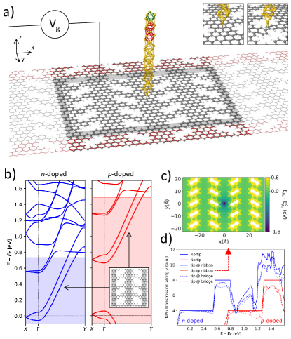
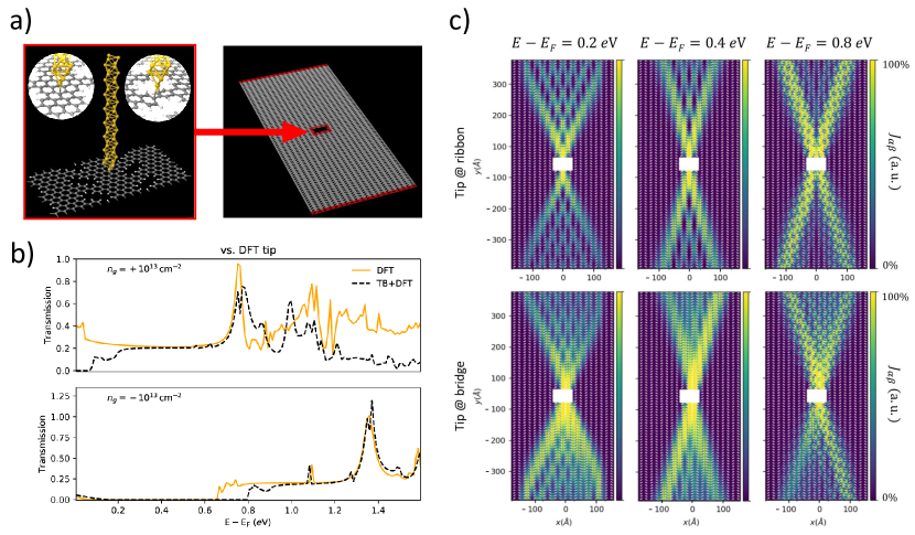
We carry out transport calculations based on NEGF Brandbyge et al. (2002); Datta (2000) applied to DFT or TB models, using TranSiesta, TBtrans Soler et al. (2002); Papior et al. (2017) and sisl Papior (2018). While parameter-free DFT models limit the accessible device sizes to only a few nanometers, parameterized TB can capture basic transport features of large systems with minor chemical perturbations (e.g. metal contact or chemical hybridization). The DFT model for the NPG device, shown in Fig. 1a, covers an area of (1449 atoms). It is defined on a single- polarized basis set 111This choice guarantees enough accuracy for the purposes of this work. A complete description of the NPG electronic structure would requires more complex basis sets Moreno et al. (2018); Papior et al. (2018). and with open (periodic) boundary conditions along (). Pores are passivated with H atoms and a model Au tip is in chemical contact with the NPG, with Au-C bond-length of . In order to describe a more realistic experimental environment we include a bottom gate in the calculations. This is done by fixing spatial charge in a gate-layer placed beneath the NPG, so as to dope it by Papior et al. (2015). The device Green’s function is calculated as
| (1) |
where and are the model overlap and Hamiltonian and , called self-energies, connect the device to semi-infinite regions along (electrodes).
A self-energy allows to seamlessly connect different regions, be it infinite bulk or localized perturbations. We exploit this to embed one or more DFT-precision regions inside much larger TB models, needed to reach experimental relevant dimensions and observe interference. The central idea of this multi-scale approach is to construct the self-energy connecting orbitals of the outermost unperturbed DFT atoms (shaded frame in Fig. 1a) to a larger TB model. We obtain TB parameters from a DFT calculation of unperturbed NPG, such that the resulting model retains the interaction range of the DFT basis set, is non-orthogonal and takes into account self-consistent effects of gates and/or bias. Therefore, besides introducing local DFT-precision in the TB model, this method enables TB-based -electrode transport calculations without any fitting parameters (see Supporting Information for further details).
DFT calculations
The positions of the outermost tip atom and the nearby C atoms in the three-probe device are optimized until forces are less than . We consider two different positions of the tip, namely on top of a C atom in the middle of a ribbon or at a bridge between two C atoms linking two ribbons (see inset to Fig. 1a). In the former case the C atoms below the tip are pushed below the NPG plane, while at the bridge site the tip binds to two aromatic rings causing a slight torsion.
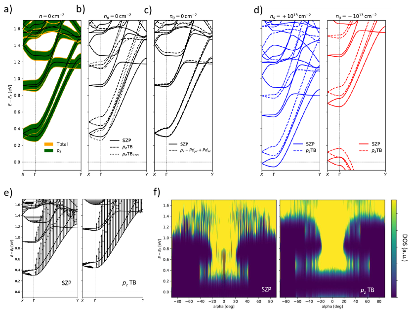
The main effect of gating on the NPG electronic structure is a rigid band shift of for - and -type doping cases, respectively (Fig. 1b). We find in both cases a band gap of between symmetric valence and conduction bands, in good agreement with results obtained for non-gated NPG Moreno et al. (2018). Bands with predominant longitudinal character are clearly visible at energies up to above (below) the conduction (valence) band (shaded areas), where states along indeed disperse more than those along . The contact with the tip causes local variation of the C potential which is screened at from the tip (Fig. 1c). This degrades transmission between the two NPG electrodes along the direction (Fig. 1d). For all energies in the longitudinal regime transport is essentially one-dimensional along the GNRs, due to the weak inter-ribbon coupling. The onset at of bands with dominant transverse character disrupts the 1D confinement and conductance quantization is lost. For all the considered gating conditions and tip positions we find qualitatively similar electronic and transport features (see Supporting Information). Below without loss of generality we mainly focus on -doped NPG probed at a ribbon site, highlighting differences only where relevant.
Multi-scale calculations
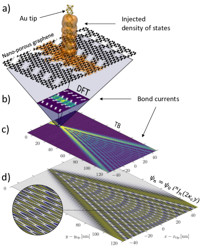
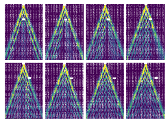
We visualize the electron flow near the contact through the injected density of states222Injected density of states is calculated by summing the absolute modules of the three eigenchannels Paulsson and Brandbyge (2007) which contribute the most to transmission from the tip to the NPG electrodes. and bond-currents from the tip,333Bond-currents are defined as , where () indicates basis orbitals centered on atom (). as shown in Fig. 5a-b. These clearly demonstrate electron confinement inside the probed ribbon up to distances comparable to the DFT cell size, for all energies ranging from the conduction band up to above it (see Supporting Information). We study the distribution of electronic current in the far-field, i.e. far from the source by performing transport calculations where the DFT “injection region” is embedded into a larger TB NPG model. We benchmark the applicability of this method by embedding the DFT-precision injection region in a TB-region which has the same boundary conditions and size of the DFT transport setup (see Supporting Information). The results show that we can reproduce the DFT transmission spectra in the longitudinal regime (Fig. 1b, shaded) by the combined DFT+TB model. Next we embed the DFT injection region as electrode in a large TB model of a device with two NPG electrodes along and a complex absorbing potential Calogero et al. (2018); Xie et al. (2014) along . This larger model reveals that at distances beyond the DFT cell size transversal losses significantly affect the far-field behavior (Fig. 5c). Current splits into neighboring ribbons with a certain periodicity of . The resulting “beams” diverge from the direction with a maximum angle which varies slightly with energy (see Supporting Information). In particular when the tip injects into a ribbon site this angle decreases from for to for . We observe similar results for injection into a bridge site, although the interference in this case is more blurred, since the injected currents start out by propagation in the two bridged ribbons (see Supporting Information).
The Talbot effect
The Talbot interference generally refers to repeated self-imaging of a diffraction grating Berry et al. (2001). In this context the wavefunction inside the element of an infinite array of weakly coupled discrete channels aligned along obeys the following discrete differential equation Yariv and Yeh (1984); Iwanow et al. (2005); Pertsch et al. (2002); Somekh et al. (1973)
| (2) |
where represents the inter-channel coupling coefficient. The coefficient can be regarded as a figure-of-merit for the degree of 1D confinement in the elements of the array: the lower the value of , the lower the spread into the weakly coupled adjacent channels. In the particular case when only a single channel is initially excited, i.e. , the solutions for Eq. (2) can be written as Yariv and Yeh (1984); Wang et al. (2017); Somekh et al. (1973)
| (3) |
where is the Bessel function of the order.
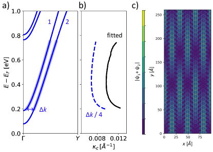
We find that the square modulus of Eq. (3) can be fitted to the far-field spectral density of states originating from the tip. The best fit on a set of -channels of a -doped NPG is illustrated in Fig. 5d. The fitted values at are and . The latter varies slightly with energy as shown in Fig. 7b. The Talbot effect originates due to interference of the two longitudinal Bloch states and . From the momentum difference one can estimate the coupling strength as Walls and Hadad (2016); Wang et al. (2017). In Fig. 7c we plot for the NPG without tip contact, showing the regular interference pattern expected when all GNRs are simultaneously excited Walls and Hadad (2016).
Dual-probe multi-scale calculations
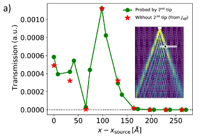
The latest developments in STM have enabled measurements with up to four tips Baringhaus et al. (2016) and control over tip-tip distance down to tens of nm Kolmer et al. (2017). Within this context, we propose to use dual-probe STM to prove the electronic Talbot effect experimentally. One probe can be used to inject current into the NPG at a fixed position as discussed above while the second probe is used to map out the interference pattern. We use the modular capability of the multi-scale approach to embed two DFT-precision tips in the large TB model. Both tips are located above NPG and we fix the probe-tip distance to around from the source. The probe-tip is moved between the bridge and ribbon positions along the white line shown in the inset in Fig. 6a. The calculated transmission between the two tips, injecting electrons at into -doped NPG, is shown in Fig. 6a. The maxima of transmission reproduce the maxima of bond-currents injected from the source in absence of the second tip within 5%. This proves that the signal in electric current detected by the second tip can map out the Talbot interference pattern.
Conclusions and outlook
In conclusion, we have explored how electrons injected by a STM probe in chemical contact to gated NPG-based devices behave in near and far field. By performing multi-scale parameter-free calculations of large-scale TB models of NPG with DFT-precision regions we found a clear signature of phase-coherence of electron waves, manifested in the far field as a Talbot interference effect. The origin of this phenomenon is the cross-talk between longitudinal 1D channels (GNRs) making up the NPG. Using proof-of-principle multi-probe calculations we have shown this interference effect may be observed in a dual-probe STM experiment. Further investigations could potentially shed light on the important impact of defects, substrate or pore functionalization on the current flow. Importantly, chemical design of the inter-ribbon bridges allows fine-tuning of the coupling strength to improve 1D transport confinement. The Talbot effect in elastic, phase-coherent transport may be used to gain insights into the phase-breaking length in these structures due to various scattering mechanisms such as electron-phonon coupling. Finally, since topologically non-trivial states were found at the edges of chiral GNRs Gröning et al. (2018); Rizzo et al. (2018), further studies might potentially reveal whether topological signatures could emerge in NPGs, perhaps impacting electron dynamics.
Acknowledgements.
Acknowledgements
Financial support by Villum Fonden (00013340), Danish research council (4184-00030), Spanish Ministerio de Economía y Competitividad (FIS2017-83780-P and MAT2016-78293-C6-4-R), UPV/EHU (IT-756-13) is gratefully acknowledged. The Center for Nanostructured Graphene (CNG) is sponsored by the Danish Research Foundation (DNRF103). We are thankful to José Caridad, Pedro Brandimarte, Isaac Alcón Rovira and Stephen Power for useful discussions.
I Supporting information
Below we provide Supporting Information on: i) Computational details; ii) DFT potential and charge distributions in gated NPG+tip systems; iii) transmission and near-field bond-currents from tip to DFT-modeled NPG; iv) multiscale method applied to NPG+tip systems; v) transmission and far-field bond-currents from DFT-precision tip to TB-modeled NPG; vi) bond-current maps from dual-probe calculations.
I.1 Computational details
The DFT electronic structure and optimized geometry for the NPG unit cell, with alternate and bridge environment as in Moreno et al. Moreno et al. (2018), are obtained using the TranSiesta code Soler et al. (2002); Papior et al. (2017). The unit cell is orthogonal and contains 100 atoms (80 C + 20 H). We use a SZP basis set with Ry energy shift. This choice neglects the existence of high-energy SAMO states, usually captured by more accurate basis sets Moreno et al. (2018). However, since the Talbot effect occurs at much lower energies, the computationally more efficient SZP basis guarantees sufficient accuracy. We use norm-conserving Troullier-Martins pseudopotentials with a mesh cutoff of Ry and the PBE Perdew et al. (1996) flavour of the generalized gradient approximation (GGA) for the exchange-correlation functional. The Brillouin zone is sampled using a Monkhorst-Pack k-point mesh. Structural optimization is performed using a force threshold of . The geometry of the tip has been optimized so as to ensure a flat density of states over the range of energies relevant for this study.
We run zero-bias DFT-NEGF calculations with TranSiesta for a three-probe device where the model tip, semi-infinite along the out-of-plane direction , is placed above the NPG, in atomic contact with it above a “ribbon” or “bridge” site. We use a NPG supercell (1449 atoms, ), periodic along the transverse direction and with two semi-infinite electrodes (top and bottom) along the longitudinal direction . Contrary to the device setup reported in Moreno et al. (2018), here we use semiconducting NPG electrodes rather than metallic pristine graphene ones. We use k-points to run the NPG+tip self-consistent calculation with TranSiesta and use k-points to compute transmission among the three electrodes with TBtrans. We set up a gate by placing a fixed charged layer below NPG such as to induce an electron density in it. This is important to pin the Fermi level in NPG electrodes and device DFT calculations. In this way we avoid artificial potential offset at the interfaces between scattering region and electrodes, which would otherwise occur due to the tip-induced change in the NPG work-function. Coordinates of the tip apex and the nearest C atoms are optimized, without gate, until forces are less than .
For the large TB+NEGF we generate NPG supercells containing up to 356.160 atoms and covering areas up to . No periodic boundary conditions are used (i.e. TBtrans -points grid includes only ). Injectced currents are drained into semi-infinite electrodes along and absorbed along using complex absorbing potentials (CAP) Calogero et al. (2018); Xie et al. (2014).
We visualize current flow in the devices plotting 2D bond-current maps, summing all bond-currents values flowing out of each atom (only positive-valued bond currents are considered). The color map is scaled in proportion to the current magnitude, so that areas with low to zero current appear in blue. Color range is normalized to the maximum value of current in the device and is often adjusted to enhance contrast.
I.2 DFT potential and charge distributions in gated NPG+tip systems
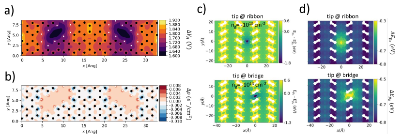
The electrostatic potential and charge distribution in the NPG are affected by application of a gate voltage as illustrated in Fig. 5a-b. Potential varies more rapidly in proximity of the narrower sections of the 7-13 GNRs. The doping charge density distribution reflects this variation, with a tendency to polarize in proximity of the regions where the potential varies the most.
Carbon levels are doped locally in the mesh when the gold STM tip is in contact with the NPG, as shown in Fig. 5c for . A maximum local -doping of and is reached depending on contact position. For the maps are very similar but the -type doping is reduced by and for the two tip positions. This is due to a higher electron population in the NPG which makes it less favorable for electrons to transfer from the tip to the NPG. As further illustrated in Fig. 5d, regardless of the tip position or the gating we always find that the doped region in proximity of the contact region extends with a radius . This proves that the supercell we use is large enough to ensure an unperturbed potential in its outermost regions.
I.3 Transmission and near-field bond-currents from tip to DFT-modeled NPG
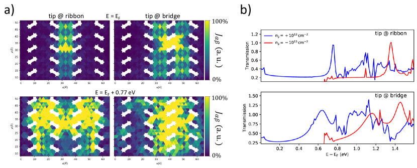
In order to visualize the current flow in the 2D mesh we calculate bond-currents among the NPG atoms while injecting electrons with various energies from the tip, as illustrated in Fig. 6a. We find that, at least up to distances comparable to the cell size, electron injected at the Fermi level or up to above it will flow within the same ribbon where they are injected. When the tip is at bridge site the situation is similar but the injected currents propagate in both the two ribbons connected by the probed bridge. At around currents start to spread across the bridges and propagate in the neighbor ribbons, as suggested by the marked spike in the transmission of Fig. 6b. At higher energies crosstalk between neighbor periodic images of the tip makes it hard to visualize the correct current flow in the system.
In Fig. 6b we plot the transmission spectra for electrons traveling from the gold tip to the two NPG electrodes. For all energies up to above the lowest unoccupied band transmission is quite constant if the tip lies in the middle of a ribbon, whereas it slowly increases when it lies at a bridge site. The onset of transversal bands at higher energies complicates the spectra significantly.
I.4 Multi-scale method applied to NPG+tip systems
Below we just highlight a few additional aspects of the multi-scale DFT+TB method applied in the context of this work.
The main idea of the approach is to transfer relevant information about electron transport between two different models by constructing a special self-energy term which connects them.
The typical protocol applied to study NPG+tip systems, relying on the versatility of sisl, is: i) setup a DFT model of the contact between NPG and a STM tip; ii) compute the self-energy which connects all C orbitals in the outermost unperturbed area of the DFT cell to all the other orbitals in it; iii) construct a large TB model by projecting a pristine DFT Hamiltonian onto the C orbitals; iv) incorporate the self-energy locally into this TB model as an extra electrode.
One important requirement is that the DFT cell containing NPG and tip is large enough to have an unperturbed potential in its outermost regions, which is where the self-energy needs to be projected. Another important requirement is that the TB model is as compatible as possible to the DFT model. This is accomplished by defining the TB parameters directly as the elements in the DFT Hamiltonian and overlap associated to the main orbitals governing transport in the energy range of interest. For the NPG case, analysis of the various orbital contributions to the DFT bandstructure reveals that longitudinal bands are predominantly dominated by carbons orbitals (Fig. 7a). The NPG bandstructure obtained with this parametrized TB model is similar to that from DFT, short of some rescaling (Fig. 7b). For example the TB first unoccupied band is shifted almost rigidly above the DFT one. Compared to a typical nearest-neighbor TB model for graphene with hopping , the parametrized model used here is non-orthogonal and the range of interaction between TB sites extends as much as in the DFT basis set. Nevertheless such a simplified model also yields bands which compare qualitatively to DFT (Fig. 7b). Such similarity, although not good enough for embedding a DFT-precision region via a self-energy (which is intrinsically non-orthogonal), suggests that it can be used a simple toy-model for NPG. The differences between parametrized TB model and DFT can be entirely attributed to pruning of the DFT basis set. In fact, although orbitals almost entirely define DFT bands and govern transport across the system, there are other orbitals in the basis which have a similar symmetry to , such as the polarized and . These would normally hybridize to some extent and give rise to deviations in the bands. These deviations can be accounted for by incorporating these few extra orbitals into a multi-orbital TB model (Fig. 7c). Application of a gate affects the TB bands the same way as the DFT ones (Fig. 7d).
Analysis of the bands velocity vectors (Fig. 7e) confirms the predominantly longitudinal or transversal nature of the electronic states as a function of energy, both for the DFT and TB models. Like the current maps reported in Fig. 7c this seems to corroborate the hypothesis of complete electron confinement within individual ribbons. However a closer look to the density of states in the NPG (see Fig. 7f) reveals that states in the longitudinal regime do not all propagate along the longitudinal direction, but rather their angle of propagation distributed over (regardless the particular DFT or TB nature of the model used to describe them). Such finite angular distribution impacts on the far-field behavior of electrons in NPG.
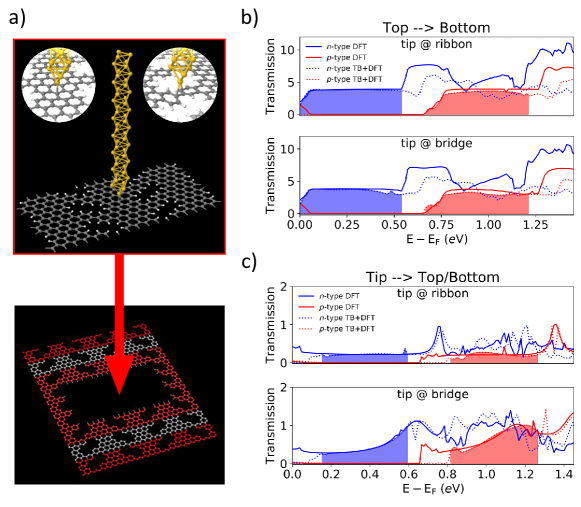
We benchmark the applicability of the multi-scale method by inserting the DFT precision injection region inside a geometry which has the same size and boundary conditions of the DFT setup (open along the longitudinal direction and periodic along the transverse) (Fig. 8a). The results in Fig. 8b-c show that we can reproduce the DFT transmission among the three electrodes over most of the longitudinal energy range by the combined DFT+TB model within accuracy. In general we find smaller deviations between DFT and DFT+TB when NPG is -doped and when the STM tip is located at a ribbon site. This trend can be attributed to the fact that the bridge site probed by the tip is too close to the outermost region where the connecting self-energy is projected (see Fig. 5c), thus preventing an optimal match between the outermost DFT potential and the external TB regions. Deviations are expected to be smaller for larger DFT supercell cell sizes. Conclusively the comparison presented here confirms that the electronic structure of DFT+TB are in very good agreement with the DFT ones, both in terms of bands shape and velocities (see Fig. 5c), despite the band-misalignment and rescaling caused by orbital-projection of the DFT Hamiltonian (see Fig. 5c).
I.5 Transmission and far-field bond-currents from DFT-precision tip to TB-modeled NPG
We introduce the DFT injection region into a larger TB model of a device with 2 bulk NPG electrodes (Fig. 9a). The transmission spectra from tip to the two large NPG electrodes compare well to DFT (Fig. 9b), regardless the particular gated conditions or tip position (only ribbon tip position is shown). Deviations can be attributed to the aforementioned pruning-induced bands rescaling.
We find that the interference pattern maximum divergence angle varies slightly with energy (Fig. 9c). For -doped NPG and tip located on a ribbon, for example, it decreases from for to for . This is in agreement with the angle-resolved density of states (Fig. 7f) and the energy dependence of the Talbot coupling strength reported in the main text. At around electrons wavelength becomes comparable to the ribbons width () hence a finer structure appears. Similar results are observed when the injection occurs in proximity of a bridge connecting two neighboring ribbons, although the interference pattern in this case is more blurred. Based on the bond currents of Fig. 6b, we interpret this as an overlap between currents which are almost equally injected into the two ribbons connected by the two probed bridge atoms.
References
- Chen et al. (2018) L. Chen, Y. Zhang, G. Chen, and I. Franco, Nature Communications 9, 2070 (2018).
- Biele et al. (2017) R. Biele, C. A. Rodríguez-Rosario, T. Frauenheim, and A. Rubio, npj Quantum Materials 2, 38 (2017).
- Karra et al. (2016) M. Karra, K. Sharma, B. Friedrich, S. Kais, and D. Herschbach, The Journal of Chemical Physics 144, 094301 (2016).
- Prindle et al. (2011) A. Prindle, P. Samayoa, I. Razinkov, T. Danino, L. S. Tsimring, and J. Hasty, Nature 481, 39 (2011).
- Brandimarte et al. (2017) P. Brandimarte, M. Engelund, N. Papior, A. Garcia-Lekue, T. Frederiksen, and D. Sánchez-Portal, The Journal of Chemical Physics 146, 092318 (2017).
- Pedersen et al. (2008) T. G. Pedersen, C. Flindt, J. Pedersen, N. A. Mortensen, A.-P. Jauho, and K. Pedersen, Physical Review Letters 100, 136804 (2008).
- Bai et al. (2010) J. Bai, X. Zhong, S. Jiang, Y. Huang, and X. Duan, Nature Nanotechnology 5, 190 (2010).
- Moreno et al. (2018) C. Moreno, M. Vilas-Varela, B. Kretz, A. Garcia-Lekue, M. V. Costache, M. Paradinas, M. Panighel, G. Ceballos, S. O. Valenzuela, D. Peña, and A. Mugarza, Science 360, 199 (2018).
- Caridad et al. (2018) J. M. Caridad, G. Calogero, P. Pedrinazzi, J. E. Santos, A. Impellizzeri, T. Gunst, T. J. Booth, R. Sordan, P. Bøggild, and M. Brandbyge, Nano Letters 18, 4675 (2018).
- Chen et al. (2016) S. Chen, Z. Han, M. M. Elahi, K. M. M. Habib, L. Wang, B. Wen, Y. Gao, T. Taniguchi, K. Watanabe, J. Hone, A. W. Ghosh, and C. R. Dean, Science 353, 1522 (2016).
- Caridad et al. (2016) J. M. Caridad, S. Connaughton, C. Ott, H. B. Weber, and V. Krstić, Nature Communications 7, 12894 (2016).
- Bøggild et al. (2017) P. Bøggild, J. M. Caridad, C. Stampfer, G. Calogero, N. R. Papior, and M. Brandbyge, Nature Communications 8 (2017).
- Xu et al. (2018) H. Y. Xu, G. L. Wang, L. Huang, and Y. C. Lai, Physical Review Letters 120, 124101 (2018).
- Allen et al. (2015) M. T. Allen, O. Shtanko, I. C. Fulga, A. R. Akhmerov, K. Watanabe, T. Taniguchi, P. Jarillo-Herrero, L. S. Levitov, and A. Yacoby, Nature Physics 12, 128 (2015).
- Silveiro et al. (2015) I. Silveiro, J. M. P. Ortega, and F. J. G. de Abajo, Light: Science & Applications 4, e241 (2015).
- Bhandari et al. (2016) S. Bhandari, G.-H. Lee, A. Klales, K. Watanabe, T. Taniguchi, E. Heller, P. Kim, and R. M. Westervelt, Nano Letters 16, 1690 (2016).
- Tetienne et al. (2017) J. P. Tetienne, N. Dontschuk, D. A. Broadway, A. Stacey, D. A. Simpson, and L. C. Hollenberg, Science Advances 3, e1602429 (2017).
- Kolmer et al. (2017) M. Kolmer, P. Olszowski, R. Zuzak, S. Godlewski, C. Joachim, and M. Szymonski, Journal of Physics: Condensed Matter 29, 444004 (2017).
- Talbot Esq. F.R.S. (1836) H. F. Talbot Esq. F.R.S., The London, Edinburgh, and Dublin Philosophical Magazine and Journal of Science 9, 401 (1836).
- Berry et al. (2001) M. Berry, I. Marzoli, and W. Schleich, Physics World 14, 39 (2001).
- Iwanow et al. (2005) R. Iwanow, D. A. May-Arrioja, D. N. Christodoulides, G. I. Stegeman, Y. Min, and W. Sohler, Physical Review Letters 95, 053902 (2005).
- Chen et al. (2015) Z. Chen, Y. Zhang, and M. Xiao, Optics Express 23, 14724 (2015).
- Walls and Hadad (2016) J. D. Walls and D. Hadad, Scientific Reports 6, 1 (2016).
- Wang et al. (2017) L. Wang, Y. Jia, and Z. Ji, Applied Optics 56, 9998 (2017).
- Solak et al. (2011) H. Solak, C. Dais, and F. Clube, Optics Express 19, 10686 (2011).
- Birnbacher et al. (2016) L. Birnbacher, M. Willner, A. Velroyen, M. Marschner, A. Hipp, J. Meiser, F. Koch, T. Schröter, D. Kunka, J. Mohr, F. Pfeiffer, and J. Herzen, Scientific Reports 6, 24022 (2016).
- Brandbyge et al. (2002) M. Brandbyge, J.-L. Mozos, P. Ordejón, J. Taylor, and K. Stokbro, Physical Review B 65, 165401 (2002).
- Datta (2000) S. Datta, Superlattices and Microstructures 28, 253 (2000).
- Soler et al. (2002) J. M. Soler, E. Artacho, J. D. Gale, A. García, J. Junquera, P. Ordejón, and D. Sánchez-Portal, Journal of Physics: Condensed Matter 14, 2745 (2002).
- Papior et al. (2017) N. Papior, N. Lorente, T. Frederiksen, A. García, and M. Brandbyge, Computer Physics Communications 212, 8 (2017).
- Papior (2018) N. R. Papior, “sisl: v0.9.5,” (2018).
- Note (1) This choice guarantees enough accuracy for the purposes of this work. A complete description of the NPG electronic structure would requires more complex basis sets Moreno et al. (2018); Papior et al. (2018).
- Papior et al. (2015) N. Papior, T. Gunst, D. Stradi, and M. Brandbyge, Physical Chemistry Chemical Physics 18 (2015).
- Note (2) Injected density of states is calculated by summing the absolute modules of the three eigenchannels Paulsson and Brandbyge (2007) which contribute the most to transmission from the tip to the NPG electrodes.
- Note (3) Bond-currents are defined as , where () indicates basis orbitals centered on atom ().
- Calogero et al. (2018) G. Calogero, R. N. Papior, P. Bøggild, and M. Brandyge, Journal of Physics: Condensed Matter 30, 364001 (2018).
- Xie et al. (2014) H. Xie, Y. Kwok, F. Jiang, X. Zheng, and G. Chen, The Journal of Chemical Physics 141, 164122 (2014).
- Yariv and Yeh (1984) A. Yariv and P. Yeh, Optical Waves in Crystals. Propagation and Control of Laser Radiation. (Wiley Series in Pure and Applied Optics, New York, 1984).
- Pertsch et al. (2002) T. Pertsch, T. Zentgraf, U. Peschel, A. Bräuer, and F. Lederer, Physical Review Letters 88, 093901 (2002).
- Somekh et al. (1973) S. Somekh, E. Garmire, A. Yariv, H. L. Garvin, and R. G. Hunsperger, Applied Physics Letters 22, 46 (1973).
- Baringhaus et al. (2016) J. Baringhaus, M. Settnes, J. Aprojanz, S. R. Power, A. P. Jauho, and C. Tegenkamp, Physical Review Letters 116, 186602 (2016).
- Gröning et al. (2018) O. Gröning, S. Wang, X. Yao, C. A. Pignedoli, G. B. Barin, C. Daniels, A. Cupo, V. Meunier, X. Feng, A. Narita, K. Müllen, P. Ruffieux, and R. Fasel, Nature 560, 209 (2018).
- Rizzo et al. (2018) D. J. Rizzo, G. Veber, T. Cao, C. Bronner, T. Chen, F. Zhao, H. Rodriguez, S. G. L. M. F. Crommie, and F. R. Fischer, Nature 560, 204 (2018).
- Perdew et al. (1996) J. P. Perdew, K. Burke, and M. Ernzerhof, Phys. Rev. Lett. 77, 3865 (1996).
- Papior et al. (2018) N. R. Papior, G. Calogero, and M. Brandbyge, Journal of Physics: Condensed Matter 30, 25LT01 (2018).
- Paulsson and Brandbyge (2007) M. Paulsson and M. Brandbyge, Phys. Rev. B 76, 115117 (2007).