Magnetic-state controlled molecular vibrational dynamics at buried molecular-metal interfaces
Abstract
Self-assembled molecular structures have been intensively used in molecular electronics and spintronics. However, detailed nature of the interfaces between molecular layers and extended metallic contacts used to bias the real devices remains unclear. Buried interfaces greatly restrict application of standard techniques such as Raman or scanning electron microscopies. Here we introduce low frequency noise spectroscopy as a tool to characterize buried molecular-metal interfaces. We take advantage of vibrational heating of the molecules with incomplete contacts to the interface. Electrons, being the main spin and charge carriers propagating through the interfaces involving self-assembled molecules, interact inelastically with charged atomic ions. Such interactions produce quantum molecular vibrations (phonons). Detailed investigation of both conductance and conductance fluctuations in magnetic tunnel junctions with few nm Perylenetetracarboxylic dianhydride (PTCDA) allows to map vibrational heating at specific biases taking place in “hot spots” where self-assembled layers weaker contact the metallic electrodes. We follow this effect as a function of PTCDA thickness and find the best molecular-metal order for the lowest (3-5 monolayers) barriers. Moreover, we unveil interplay between spin and phonons at interface showing experimentally and by modelling spin-control over molecular vibrational heating. We find that vibrational heating related low frequency noise essentially depends on the relative alignment of the electrodes with noise changes well beyond expectations from fluctuation-dissipation theorem.
I Introduction
Downscaling of inorganic electronics has currently become increasingly difficult because of physical limitations, due to surface-related modification of the electronic structures. The bottom-up concept introduced by molecular electronics in order to solve the problem has been around since the seventies Mann1971 and unique intrinsic features of molecules and quantum dots, among other excited phonons and vibrations Nitzan2003 ; Galperin2007 ; Kennehan2018 , have been explored intensively.
One of the major challenges in molecular electronics (molecular spintronics) is control over of molecules-metal (ferromagnetic electrodes) contacts Chen2018 . To avoid possible damage to molecular order and even pin-hole formation a deposition of seed under-oxidized atomic thick Alumina layer has been proposed Santos2007 . This method both improves interface quality, reduces influence of conductance mismatch and enhances spin life time Santos2007 ; Li2011 . However, as long as one deals with buried interfaces, the tools available to evaluate their quality are very limited. For such purpose (when electron transmission microscopy is used Wiktor2017 ) the device is usually destroyed.
Electron transport through the interfaces could be a non-destructive, albeit indirect method to evaluate buried molecule-metal interface quality. Few main factors determine transport in molecular electronics, with electron-phonon coupling being of importance along with molecular and electrodes electronic structures Galperin2005 ; Ward2011 ; Elliott2012 . The identification of phonon modes is usually carried out by Raman or inelastic tunneling spectroscopy (IETS) Elliott2012 ; Galbiati2015 . Due to strong photon attenuation by the metallic electrodes, Raman spectroscopy on heterostructures mainly reflects information from the out surface layers Tan2017 .
The IETS technique, based on a weak change in the tunneling conductance beyond the vibrational onsets of excitation, is mostly used to explore molecular vibrations in the single-molecule limitStipe1998 ; Smit2002 and when contacted by sharp tips with undefined magnetization direction. For the organic magnetic tunnel junctions, the conductance signals are averaged over a large number of molecules forming either barrier or contacting extended ferromagnetic electrodes. To our best knowledge, the only study of the IETS in molecular spintronics just aimed to obtain structural information on the integrity of the barrier by localizing junctions with pin-holes where no signatures of molecular vibrational modes were present Galbiati2015 . As we shall see below, for the high quality buried molecular-metal interfaces with only small percentage on the molecules weakly contacting the electrode, the detailed investigation of the buried molecule-metal interfaces could be carried out by analyzing vibrational heating of the molecules in locally distributed “ hot spots”.
Vibrational heating (or cooling) of the molecules contacting metal electrodes is a well established phenomenon Dubi2011 for atomic and molecular junctions. Vibrational heating at finite bias is among the major obstacles for advances in molecular electronics and spintronics due to the associated potential device breakdown Dubi2011 ; Simine2012 ; Galperin2007 ; Weiss2015 . Peculiarly, as mentioned above, a current flux can either heat or cool locally the molecular junction close to sub-vibration resonance conditions Galperin2009 ; Simine2012 .
The inclusion of the electron spin degree of freedom in organic magnetic tunnel junctions (OMTJs)Dediu2002 ; Xiong2004 ; Rocha2005 ; Santos2007 ; Sanvito2011 ; Jian2011 ; Vincent2012 ; Nguyen2012 ; Rakh2016 and interface-related molecular magnetism Sanvito2010 ; Lach2012 potentially allows spin control over vibrons, as pointed out in recent theoretical studies Droghetti2015 ; Lunghi2017 . Other theories go even further and predict phonon-dressed spins to exist with effective magnetic moments of for single-phonon quanta with the original system being non-magnetic Shin2018 . The interplay between spins and phonons in molecular spintronics remains however obscured.
As we shall see below, the conductance fluctuations or inelastic noise probing vibron excitations could present an alternative tool capable of identifying high quality buried molecules-metal interfaces. At low temperatures and biases not yet exciting molecular vibrations or defect states, (e.g. typically below 10mV) voltage fluctuations are dominated by shot noise providing information on interfacial electron-electron correlations Cascales2014 . At higher biases (typically exceeding phonon energies situated above 15mV), the low-frequency noise (LFN) is known to provide unique capability of identifying surface located molecules through their vibrations in non-spintronic systems Tsutsui2010 ; Schaffert2012 .
Here we describe qualitative step further and introduce vibron noise spectroscopy, which addresses the challenge of investigation of quality of buried molecular-metal (ferromagnet) interfaces in OMTJs. Our experiments monitor conductance, tunneling magnetoresistance and voltage fluctuations as a function of applied bias and magnetic state in the OMTJs with efficient heat transport away from the molecules so that the junction’s structure is not jeopardized. The junctions with thinnest (3-5 PTCDA monolayers) barrier show the smallest background noise and highest TMR of 20-30 indicative of their major structural order. In those junctions, we experimentally observe and theoretically model the spin-dependent molecular vibrational dynamics. The physical origin of this effect is related to the difference of available phase space for the inelastic tunneling process between parallel and antiparallel states. Besides, our results open the possibility of spin heat-dissipation control in molecular spintronics.
II Results
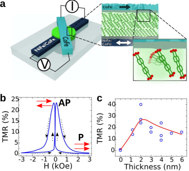
The sample growth and measurement technique are explained in the Methods section. More details could be found in Refs Li2011 ; Hong2014 ; Herranz2010 ; Cascales2014 . Figure 1 illustrates the investigated OMTJs highlighting the 1.2 nm thick barrier cross-section (with approximately three layer of PTCDA). The sketched molecular order (zoom in Fig. 1a) describes a realistic PTCDA structure with some conductance channels at zero bias being open due to molecular bending, interface roughness or local disorder.
An exponential dependence of the room temperature conductance with the PTCDA thicknessCascales2014 and a large tunneling magnetoresistance (TMR) (Fig. 1b,c) indicate that the electron transport through the PTCDA layer is dominated by direct tunneling with energy and spin relaxation close to the molecule/ferromagnet interfaces. Figure 1b shows two well-defined and reproducible magnetic states corresponding to parallel (P) and close to antiparallel (AP) alignment of the electrodes. Tunneling magnetoresistance values (up to ) observed with below 2nm thick PTCDA barriers (3-5 monolayers) are among the highest reported so far in molecular spintronic junctions in the tunneling regime. High TMR signals well ordered self-assembled thinnest PTCDA barrier. Conductance and noise in a total of 13 samples were investigated with PTCDA thickness ranging from 0 to 6 nm. Unless otherwise indicated, the measurements temperature is 10K.
Figures 2a-c describe representative behavior of noise for OMTJs with PTCDA thickness of 1.2 nm in two magnetic states. These junctions show the lowest contribution to the noise signalling a higher molecular order. One observes unexpected enhancement of the noise power due to appearance of random telegraph noise (RTN) in conductance close to set of specific biases. Qualitatively similar magnetic state dependent LFN has been found when the measurements are carried out at base temperature of K (Fig. S1, Ref.SupMaterial ). The close to symmetric character of the LFN anomalies with voltage points towards a vibrational origin rather than to a resonant electron tunneling process, for which LFN enhancement is expected for one bias polarity only Clement2007 .
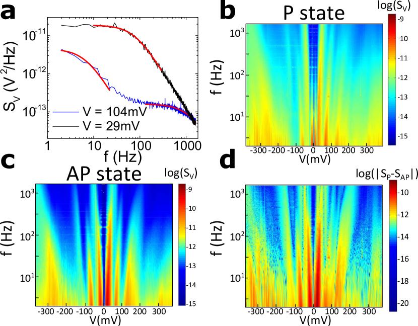
In order to analyze in detail the shape and symmetry of the RTN on bias, the observed effect has been represented in two qualitatively different plots. From the one side, Fig. 2b shows rough data, i.e., the variation of the noise power in the parallel state () with frequency and the applied bias. On the other hand, we have quantified how RTN characteristic frequency varies with applied bias and its polarity. As example, Fig. 2a shows cross-sections of from the Figure 2b for the two particular biases close revealing specific RTN humps. With increasing bias, the RTN first appears as a noise excess in the low-frequency limit which approximately varies as with being the characteristic RTN frequency. This quantitative analysis confirms that set of specific RTN excitations is nearly symmetric in bias and shows an increase of the under the applied bias before RTN disappears outside the experimental bandwidth. Some asymmetry could probably be related with differences in the bottom and top electrode roughness and electrode/barrier interface.
Interestingly, switching the device with clear LFN anomalies (here with PTCDA as we shall see below) to the AP state substantially changes the LFN (Fig. 2c). In order to quantify the net change in LFN between the two magnetic states we calculate the absolute value of the difference of the noise power between P and AP states (Fig. 2d). Note that for the both magnetic states and at biases exceeding 200 mV the RTN anomalies appear to be smeared out. As see in Fig. 2b,c and specially for OMTJs with yet thicker PTCDA, in the high-bias range the so-called background noise becomes superimposed on the RTN contribution making it more challenging to accurately determine the RTN characteristic frequencies
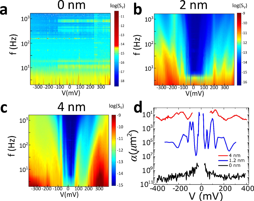
In order to understand better the nature of the observed bias and magnetic state dependent RTN, we carried out noise spectroscopy as a function of PTCDA thickness ( see Fig. 3). Let us first analyse LFN in the control samples (i.e., junctions without PTCDA but with 0.6+0.6 nm of AlOx separating two ferromagnetic electrodes). One observes practically featureless background noise (Fig. 3a) which is at least two orders in the magnitude below the LFNs measured in any of the junctions with a PTCDA barrier. We conclude that set of the bias-dependent RTN features originates from molecular vibrations inside the PTCDA barrier or at the PTCDA/electrode interfaces.
Further increase of the PTCDA thickness maintains the well-defined bias dependent RTN anomalies only for barrier thickness below or about 2nm. We observe the clear signatures of vibron related LFN with 1.2nm and partially with 2nm PTCDA thickness only. The further increase of the PTCDA thickness (as shown for OMTJ with 4nm PTCDA) smeares out vibron related signatures in noise due to onset of the strong background 1/f noise already at relatively small biases (Fig. 3c).
To show more clear the applicability range of the vibron noise spectroscopy when following the qualitative changes in the LFN with increasing PTCDA thickness we may also use the Hooge factor explained in Methods. Fig. 3d plots the bias dependence of the Hooge factor for OMTJs with three different PTCDA thicknesses. While the control samples show a practically featureless Hooge vs. bias dependence, the introduction of 1.2 nm PTCDA (about three PTCDA layers) between two ferromagnetic electrodes raises dramatically the normalized noise (several orders of magnitude). The strongest relative LFN anomalies with bias were observed for the 1.2-2 nm thick PTCDA barriers (Fig. 3b,d). A further increase of the PTCDA thickness boosts the LFN background, approaching the LFN spectrum closer to the type. This induces a relative decrease of the magnitude of LFN anomalies, as seen for the OMTJs with 4 nm thick PTCDA. Generally, the evolution of LFN with PTCDA points towards a predominantly interfacial origin of the LFN anomalies, gradually affected by the accumulation of molecular disorder with an increasing barrier thickness.
It is important to note that spin-dependent molecular vibron noise (Fig. 2) in few orders of the magnitude exceeds in the noise power expected from the application of fluctuation-dissipation theorem (FDT). Indeed, from FDT the thermal noise power is Alievbook2018 (with being temperature, - junction resistance and - Boltzmann contant). Then below 10K with measured resistance change between P and AP state of few kOhm, the noise power change expected from FDT should be less than . The experimentally observed variation of the noise power between P and AP states (see Figs. 2d) exceeds that by more than six orders of the magnitude.
Concerning the robustness of the bias-dependent RTN anomalies in each magnetic state we have carried out a number of reproducibility tests. The corresponding analysis shown in Fig. S2 (Ref.SupMaterial ) permits to conclude that the RTN vs. bias anomalies are rather reproducible.
Interestingly, the enhancement of the LFN power at specific biases (up to several orders of the magnitude) is accomplished with limited impact (with relative change below ) on the bias-dependent conductance (Fig. S3, Ref.SupMaterial ). This suggests that a great majority of the molecular conductance channels in our OMTJs arise from well-established contacts between molecules and the electrodes. At the same time, only a small fraction of the total conductance channels (roughly estimated to be from the relation between square root of the integrated over experimental bandwidth voltage noise power to the applied bias) contribute to the RTN as schematically sketched in Fig. 1a.
III Discussion
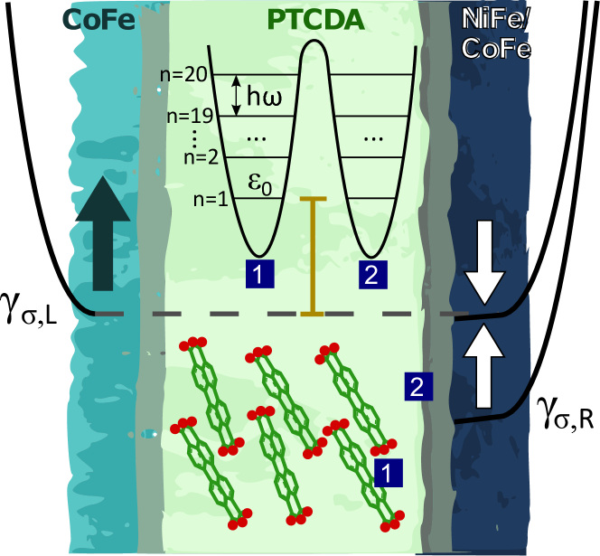
Based on this scenario, we consider below a simple model of the barrier in which a molecular conduction pathway can attain two different states, e.g., due to unavoidable interface roughness (Fig. 4). The configuration becomes unstable under applied bias and switching between, for example, straight and bended molecular conformal configurations may occur. The stable conduction pathways (in parallel) contribute only to the background signal and provide practically a featureless noise. We therefore suggest that the observed excess of the RTN above certain characteristic biases is a result of inelastic excitations and conformational switching of individual molecules (or collective groups) in the barrier.
Following Refs. Gao1997, ; Brumme2012, ; Frederiksen2014, we generalize a model for a two-state switch driven by inelastic excitations by a spin-polarized electronic current with main parameters described in Fig. 4, the main text and detailed in SM SupMaterial . Interestingly, this model predicts that the reaction yield, i.e., the probability that a tunneling electron induces the reaction, is larger in the P than in the AP electrode configuration (Fig. S6). The origin of this effect is related to the available phase space (initial and final states) for the inelastic tunneling process which is larger in P than in AP. This is analogous to the TMR effect where the elastic transmission of electrons is also larger in P than AP. We note that these two effects compound in the reaction rate (Eq. S19, Ref.SupMaterial ).
To link these findings to the experimental observations we present in Fig. 5 an application of the model with appropriately chosen parameters. As detailed in the SM SupMaterial we consider the metal-molecule-metal tunnel junction as described by a single electronic resonance bridging two metal electrodes with coupling of the electrons to a set of vibrational modes on the molecular bridge. The numerical results shown in Fig. 5 were obtained with the following model parameters defined in the SI: eV, and meV. The molecular vibrations were described by a set of modes characterized by energies being multiples of meV. The electrode polarization was defined phenomenologically as . The resulting TMR and LFN spectrum were computed using Eqs. S22 and S26, respectively, with the switching rate given by Eq. S19 (Ref. SupMaterial ).
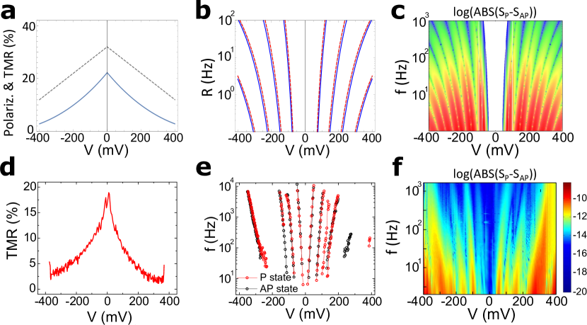
Figure 5a shows the electrode polarization (dashed gray curve) and TMR (blue curve), where the latter describes well the typical experimental voltage dependence of the TMR (Fig. 5d). For simplicity we represent the molecular vibrations by a set of modes characterized by energies being multiples of meV. At a given applied voltage this translates into a set of characteristic switching rates as shown in Fig. 5b, qualitatively similar to the experimental data in Fig. 5e. Finally, we analyze the magnetic-state dependent noise spectrum for realistic bias-dependent TMRs and associated spin polarizations. By the eye it is hard to appreciate the difference by P or AP (Fig. 5b,e and Fig. S4, Ref. SupMaterial ). The difference only becomes apparent when one considers the quantity as shown in 5c, in some resemblance with the experimental data in 5f. We thus deduce that our modeling qualitatively can reproduce the main experimental observations.
In summary, we have introduced low frequency noise spectroscopy as a tool to characterize buried organic-metal interfaces. Key sensors for this spectroscopy are ”hot spots” where molecular vibrational heating induces random telegraph noise detectable by standard noise measurement techniques. Moreover, we experimentally demonstrate and describe by the simple model the spin control of vibrational dynamics and switching in molecular spintronic devices. Our findings suggest the main LFN mechanism in molecular tunnel junctions with relatively ordered thin barriers and buried interfaces and therefore important for the development of reliable molecular spintronic devices.
IV Methods
IV.1 Sample growth
The layer sequence in the PTCDA organic spin valves studied in this work is: NiFe(25 nm)/CoFe(15 nm)/AlxO(0.6 nm)/PTCDA(1.2-5 nm)/AlxO(0.6 nm)/CoFe(30 nm). The structure was deposited onto a glass substrate, and the junctions were prepared in a high-vacuum environment with a base pressure lower than mbar. The metallic layers were deposited by sputtering with an Ar working pressure of mbar. The PTCDA layers were grown by thermal evaporation at mbar, with a deposition rate of 0.1 nm/s. Thin AlOx layers were grown between the PTCDA layer and both ferromagnetic layers by partially oxidizing Al in an oxygen plasma for 5 s.
IV.2 Electron transport and noise measurements
Electron transport and noise were measured down to 0.3 K using a He-3 JANIS cryostat. LFN experiments were carried out using a Stanford Research SR785 spectrum analyzer. The signal is duplicated into two channels identically amplified in two stages in order to use a cross-correlation technique so we may neglect extrinsic voltage noise contributions. We analyze the variation of LFN by direct plots of the noise power. For the qualitative comparison of the frequency-averaged LFN levels in our OMTJs with PTCDA barrier thickness we also used the Hooge factor definedHerranz2010 via where is the bias voltage, the junction area, the frequency, and a parameter close to 1.
V Acknowledgements
We thank Juan Carlos Cuevas for stimulating discussions and constructive comments. The work in Madrid has been supported by Spanish MINECO (MAT2015-66000-P and EUIN2017-87474), Comunidad de Madrid (NANOFRONTMAG-CM S2013/MIT-2850) and IFIMAC (MDM-2014-0377). TF acknowledges FIS2017-83780-P from the Spanish MINECO. We also gratefully acknowledge support by UAM-Santander collaborative project (2015/ASIA/04). J.P.C. acknowledges support from the Fundacion Seneca (Region de Murcia) postdoctoral fellowship (19791/PD/15)
† These authors contributed equally
References
- (1) B. Mann and H. Huhn, Tunneling through Fatty Acid Salt Monolayers, J. Appl. Phys. 42, 4398 (1971).
- (2) A. Nitzan and M. A. Ratner, Electron Transport in Molecular Wire Junctions, Science 300, 1384 (2003).
- (3) M. Galperin, M. A Ratner and A. Nitzan, Molecular transport junctions: vibrational effects, J. Phys.: Condensed Matter 19, 103201 (2007).
- (4) E.R. Kennehan, G.S. Doucette, S. Grayson, A.R. Marshall, R. Ashley, C. Grieco, K.T. Munson, T. Kyle, M.C. Beard, C. Matthew, J.B. Asbury, Electron-Phonon Coupling and Resonant Relaxation from 1D and 1P States in PbS Quantum Dots, ACS Nano 12, 6263 (2018).
- (5) J. Chen, H. Isshiki, C. Baretzky, T. Balashov, W. Wulfhekel, Abrupt Switching of Crystal Fields during Formation of Molecular Contacts, ACS Nano, 12, 3280 (2018).
- (6) T. S. Santos, J. S. Lee, P. Migdal, I. C. Lekshmi, B. Satpati, J. S. Moodera, Room-Temperature Tunnel Magnetoresistance and Spin-Polarized Tunneling through an Organic Semiconductor Barrier, Phys. Rev. Lett. 98, 016601 (2007).
- (7) K.-S. Li, Y.-M. Chang, S. Agilan, J.-Y. Hong, J.-C. Tai, W.-C. Chiang, K. Fukutani, P. A. Dowben and M.-T. Lin, Organic spin valves with inelastic tunneling characteristics, Phys. Rev. B 83, 172404 (2011).
- (8) C. Wiktor, M. Meledina, S. Turner, O. I. Lebedev and R. A. Fischere, Transmission electron microscopy on metal–organic frameworks – a review, Journal of Material Chemistry A, 5,14969 (2017).
- (9) M. Galperin, M.A. Ratner, A. Nitzan, Hysteresis, switching, and negative differential resistance in molecular junctions: A polaron model, Nano Lett., 5,125 (2005).
- (10) D. R. Ward, D. A. Corley, J. M. Tour and D. Natelson, Vibrational and electronic heating in nanoscale junctions, Nature Nanotechnology 6, 33 (2011).
- (11) A. B. S. Elliott, R. Horvath and K. C. Gordon, Vibrational spectroscopy as a probe of molecule-based devices, Chem. Soc. Rev. 41, 1929 (2012).
- (12) M. Galbiati, S. Tatay, S. Delprat, H. Le Khanh, B. Servet, C. Deranlot, S. Collin, P. Seneor, R. Mattana, and F. Petroff, Is spin transport through molecules really occurring in organic spin valves? A combined magnetoresistance and inelastic electron tunnelling spectroscopy study, Appl. Phys. Lett. 106, 082408 (2015).
- (13) Y. Tan, L. Ma, Z. Gao, M. Chen, F. Chen, Two-Dimensional Heterostructure as a Platform for Surface-Enhanced Raman Scattering, Nano Lett. 17, 2621 (2017).
- (14) B. C. Stipe, M. A. Rezaei, and W. Ho, Single-Molecule Vibrational Spectroscopy and Microscopy, Science 280, 1732 (1998).
- (15) R. H. M. Smit, Y. Noat, C. Untiedt, N. D. Lang, M. C. van Hemert, and J. M van Ruitenbeek, Measurement of the conductance of a hydrogen molecule, Nature 419, 906-909 (2002).
- (16) Y. Dubi and M. Di Ventra, Colloquium: Heat flow and thermoelectricity in atomic and molecular junctions, Rev. Mod. Phys. 83, 131 (2011).
- (17) L. Simine and D. Segal, Vibrational cooling, heating, and instability in molecular conducting junctions: full counting statistics analysis, Phys. Chem. Chem. Phys. 14, 13820 (2012).
- (18) S. Weiss, J. Brüggemann, and M. Thorwart, Spin vibronics in interacting nonmagnetic molecular nanojunctions, Phys. Rev. B 92, 045431 (2015).
- (19) M. Galperin, K. Saito, A. V. Balatsky, A. Nitzan, Cooling mechanisms in molecular conduction junctions, Phys. Rev. B 80, 115427 (2009).
- (20) V.A. Dediu, M. Murgia, F.C. Matacotta, C. Taliani, S. Barbanera, Room temperature spin polarized injection in organic semiconductor, Solid State Comm. 122, 181 (2002).
- (21) Z. H. Xiong, D. Wu, Z.V. Vardeny, J. Shi, Giant magnetoresistance in organic spinvalves, Nature 427, 821 (2004).
- (22) A. R. Rocha, V. M. Garcia-Suarez, S. W. Bailey, C. J. Lambert, J. Ferrer, S. Sanvito, Towards molecular spintronics, Nature Mater. 4, 335 (2005).
- (23) S. Sanvito, Molecular Spintronics, Chem. Soc. Rev. 40, 3336 (2011).
- (24) J. S. Jiang, J. E. Pearson, S. D. Bader, Direct Determination of Energy Level Alignment and Charge Transport at Metal–Alq3 Interfaces via Ballistic-Electron-Emission Spectroscopy, Phys. Rev. Lett. 106, 156807 (2011).
- (25) R. Vincent, S. Klyatskaya, M. Ruben, W. Wernsdorfer, F. Balestro, Electronic read-out of a single nuclear spin using a molecular spin transistor, Nature 488, 357 (2012).
- (26) T. D. Nguyen, E. Ehrenfreund, Z. V. Vardeny, Spin-Polarized Light-Emitting Diode Based on an Organic Bipolar Spin Valve, Science 337, 204 (2012).
- (27) D. Rakhmilevitch, S. Sarkar, O. Bitton, L. Kronik, O. Tal, Enhanced Magnetoresistance in Molecular Junctions by Geometrical Optimization of Spin-Selective Orbital Hybridization Nano Lett. 16, 1741 (2016).
- (28) S. Sanvito, Molecular spintronics: the rise of spinterface science, Nature Physics 5, 562 (2010).
- (29) S. Lach, A. Altenhof, K. Tarafder, F. Schmitt, Md. E. Ali, M. Vogel, J. Sauther, P. M. Oppeneer, and C. Ziegler, Metal–Organic Hybrid Interface States of A Ferromagnet/Organic Semiconductor Hybrid Junction as Basis For Engineering Spin Injection in Organic Spintronics, Adv. Funct. Mater. 22, 989 (2012).
- (30) A. Droghetti, I. Rungger, M. Cinchetti, and S. Sanvito, Vibron-assisted spin relaxation at a metal/organic interface, Phys. Rev. B 91, 224427 (2015).
- (31) A. Lunghi, F. Totti, R. Sessoli, S. Sanvito, The role of anharmonic phonons in under-barrier spin relaxation of single molecule magnets, Nat. Commun. 8, 14620 (2017).
- (32) D. Shin, H. Hübener, U. De Giovannini, H. Jin, A. Rubio, N. Park, Phonon-driven spin-Floquet magneto-valleytronics in MoS2, Nat. Commun. 9, 638 (2018).
- (33) J. P. Cascales, J-Y. Hong, I. Martinez, M-T. Lin, T. Szczepanski, V. K. Dugaev, J. Barnas, and F. G. Aliev, Superpoissonian shot noise in organic magnetic tunnel junctions, Appl. Phys. Lett. 105, 233302 (2014).
- (34) M. Tsutsui, M. Taniguchi, and T. Kawai, Single-molecule identification via electric current noise, Nature Commun. 1, 138 (2010).
- (35) J. Schaffert, M. C. Cottin, A. Sonntag, H. Karacuban, C. A. Bobisch, N. Lorente, J-P. Gauyacq and R. Möller, Imaging the dynamics of individually adsorbed molecules, Nature Mater. 12, 223 (2012).
- (36) J.-Y. Hong, K.-H. Ou Yang, B.-Y. Wang, K.-S. Li, H.-W. Shiu, C.-H. Chen, Y.-L. Chan, D.-H. Wei, F.-H. Chang, H.-J. Lin, W.-C. Chiang and M.-T. Lin, Interfacial spectroscopic characterization of organic/ferromagnet hetero-junction of 3,4,9,10-perylene-teracarboxylic dianhydride-based organic spin valves, Appl. Phys. Lett. 104, 083301 (2014).
- (37) D. Herranz, F. Bonell, A. Gomez-Ibarlucea, S. Andrieu, F. Montaigne, R. Villar, C. Tiusan, and F. G. Aliev, Strongly suppressed 1/f noise and enhanced magnetoresistance in epitaxial Fe–V/MgO/Fe magnetic tunnel junctions, Appl. Phys. Lett. 96, 202501 (2010).
- (38) See Supplemental Material at XXX for further details on the experimental measurements and theoretical calculations, as well as Figs. S1-S5.
- (39) N. Clement, S. Pleutin, O. Seitz, S. Lenfant, and D. Vuillaume, 1/f tunnel current noise through si-bound alkyl monolayers, Phys. Rev. B 76, 205407 (2007).
- (40) F. G. Aliev and J. P. Cascales, Noise in spintronics: from understanding to manipulation (Pan Stanford Publishing, Singapore, 2018).
- (41) S. Gao, M. Persson, and B. I. Lundqvist, Theory of atom transfer with a scanning tunneling microscope, Phys. Rev. B 55, 4825 (1997).
- (42) T. Brumme, R. Gutierrez and G. Cuniberti, Vibrational heating in single-molecule switches: an energy-dependent density-of-states approach, J. Phys.: Condens. Matter 24, 394003 (2012).
- (43) T. Frederiksen, M. Paulsson, and H. Ueba, Theory of action spectroscopy for single-molecule reactions induced by vibrational excitations with STM, Phys. Rev. B 89, 035427 (2014).