Synthetic Semimetals with van der Waals Interfaces
Abstract
The assembly of suitably designed van der Waals (vdW) heterostructures represents a new approach to produce artificial systems with engineered electronic properties. Here, we apply this strategy to realize synthetic semimetals based on vdW interfaces formed by two different semiconductors. Guided by existing ab-initio calculations, we select WSe2 and SnSe2 mono and multilayers to assemble vdW interfaces, and demonstrate the occurrence of semimetallicity by means of different transport experiments. Semimetallicity manifests itself in a finite minimum conductance upon sweeping the gate over a large range in ionic liquid gated devices, which also offer spectroscopic capabilities enabling the quantitative determination of the band overlap. The semimetallic state is additionally revealed in Hall effect measurements by the coexistence of electrons and holes, observed by either looking at the evolution of the Hall slope with sweeping the gate voltage or with lowering temperature. Finally, semimetallicity results in the low-temperature metallic conductivity of interfaces of two materials that are themselves insulating. These results demonstrate the possibility to implement a state of matter that had not yet been realized in vdW interfaces, and represent a first step towards using these interfaces to engineer topological or excitonic insulating states.
keywords:
van der Waals heterostructures, semimetal, band overlap, ionic liquid gating, 2D materialsThese two authors contributed equally \alsoaffiliationGroup of Applied Physics, University of Geneva, 24 Quai Ernest Ansermet, CH-1211 Geneva, Switzerland \altaffiliationThese two authors contributed equally \alsoaffiliationGroup of Applied Physics, University of Geneva, 24 Quai Ernest Ansermet, CH-1211 Geneva, Switzerland \alsoaffiliationGroup of Applied Physics, University of Geneva, 24 Quai Ernest Ansermet, CH-1211 Geneva, Switzerland \alsoaffiliationGroup of Applied Physics, University of Geneva, 24 Quai Ernest Ansermet, CH-1211 Geneva, Switzerland \alsoaffiliationUniversité Paris Est Creteil, CNRS, ICMPE, UMR 7182, F-94320, Thiais, France \alsoaffiliationGroup of Applied Physics, University of Geneva, 24 Quai Ernest Ansermet, CH-1211 Geneva, Switzerland
The possibility to assemble heterostructures of different two-dimensional (2D) van der Waals (vdW) materials1 without any constraint imposed by the need to match their lattices discloses unprecedented opportunities to realize artificial systems2, 3 hosting novel electronic states. Known examples include the modification of the band structure of graphene placed onto hexagonal boron nitride4, 5, 6, the drastic enhancement of spin-orbit interaction in graphene on semiconducting transition metal dichalcogenide (TMD) substrates 7, 8, 9, 10, 11, 12, the occurrence of superconductivity in twisted bilayer graphene 13, 14, 15, 16, and the appearance of correlated insulating states in gate-doped twisted TMD bilayers17, 18. Many more interesting artificial systems can be envisioned, because vdW interfaces allow 2D materials hosting distinct electronic phenomena –such as superconductivity19, 20, magnetism 21, 22, 23, 24, 25, 26, charge density waves 27, 28, 29, and more – to be brought in contact, within sub-nanometer distances.
Here we demonstrate how vdW interfaces can be used to realize synthetic semimetals, by stacking on top of each other two atomically thin semiconductors with a suitable band alignment. The strategy is similar to that employed recently to assemble vdW interfaces acting as artificial semiconductors30, 31, 32 with a controlled band-gap (see Fig. 1(a)). Realizing a semimetallic state requires the bottom of the conduction band in one of the semiconductors to be lower in energy than the top of the valence band in the other (see shaded bands profiles in Fig. 1(b)), so that the conduction and valence bands of the two materials overlap in energy. Under these conditions, charge is transferred from one material to the other, causing both bands to be partially filled. The Fermi level is then positioned in the energy interval in which the two bands overlap, turning the interface of two insulating 2D materials into a conductor, due to the simultaneous presence of electrons and holes.
Semimetals of this type are expected to exhibit interesting phenomena, depending on details of the interfacial electronic structure. If the overlapping bands of the constituent materials are both centered at the -point, for instance, the interface should host a 2D quantum spin Hall state. Indeed, in this case the situation is analogous to that of III-V InAs/GaSb heterostructures33, 34, 35, with the advantage that in vdW interfaces, the atomic thickness of the constituent 2D materials can strongly enhance wavefunction overlap and hybridization effects between the two layers, resulting in a much larger gap between the inverted bands (for this to occur, strong spin-orbit interaction needs to be present, which is the case for the 2D materials that we consider36, 37, 38). If the band overlap does not occur at the same position in -space, coupling between electrons and holes in the two layers can still occur, but is predominantly mediated by Coulomb interaction. In this regime, theory39 predicts the system to undergo a transition to an excitonic insulating state, in which electrons and holes are bound together, forming neutral excitons that do not carry current. Such an excitonic insulating state has not been observed to occur spontaneously in natural semiconducting materials, and vdW interfaces offer a new platform for its search.
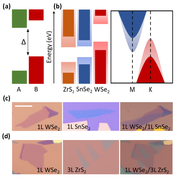
Our goal here is to show that a semimetallic state can indeed be realized in vdW interfaces formed by two different 2D semiconductors, and to demonstrate experimentally all its basic characteristic features: the presence of band overlap, the coexistence of electrons and holes, and the metallic nature of transport. Identifying suitable constituent semiconductors to assemble a semimetallic vdW interface is not straightforward, because for most semiconducting 2D materials the relative band offset is too small to bridge their band gap and create a band overlap. To guide our search, we rely on ab-initio calculations reported in the literature, discussing the electronic structure of interfaces based on combinations of monolayers of many different vdW semiconductors. In particular, the results of Zhang et al.40 and Koda et al.41 suggest that monolayers of WSe2 and SnSe2 or of WSe2 and ZrS2 should yield either a band overlap or a small band gap (see Fig. 1(b)). If sufficiently small, the presence of a gap between two monolayers does not necessarily represent a problem, because selecting bi or trilayers of these same materials can then likely allow a finite band overlap at the interface to be achieved (simply because the band gap of most 2D semiconductors under consideration decreases significantly upon increasing their thickness). These combinations of 2D materials are therefore promising to realize synthetic semimetallic systems. Nevertheless, since the precision of ab-initio calculations for the quantitative determination of material band gaps and of their band alignment is limited, it remains to be seen whether experimentally these interfaces behave as predicted theoretically (indeed, in recent work where a band overlap was expected based on theoretical predictions, no sign of a semimetallic state was found in the experiments42).
To verify experimentally the occurrence of an interfacial semimetallic state we perform different types of transport measurements. To this end, we realize devices with nano-fabricated metallic contacts attached to the interfaces, and equip them with ionic liquid gates, to allow the accumulation of very large densities of charge carriers (either electrons or holes). Thanks to their very large geometrical capacitance these devices also enable spectroscopic measurements, as we explain in more details below. Examples of exfoliated layers of WSe2, SnSe2 and ZrS2 used in our experiments are shown in Fig. 1(c) and (d), together with the images of the resulting vdW interfaces. Fig. 2 shows both the schematics of ionic liquid gated field-effect transistor (FET) devices (Fig. 2(c)) as well as optical microscope images of different interface devices with attached metallic contacts (insets of Fig. 2(d) and (e)). In practice, devices were realized using exfoliated layers of different thickness, ranging from monolayer (1L) to six-layers (6L) (the sources of the bulk crystals used for exfoliation are listed in the supplementary information). Exfoliation and interface assembly were done with the aid of a motorized stage in a nitrogen-filled glove box ( 0.1 ppm O2 and H2O) in order to avoid any material deterioration (for ZrS2 this is essential, as processing this material in air causes substantial degradation). The procedures used to assemble the interfaces, to attach contacts, and to apply the ionic liquid (P14-FAP) are by now rather conventional and are described in detail in the supplementary information.
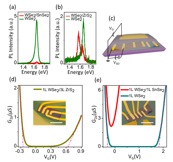
As a first characterization step, for some of the as-assembled interfaces we performed photoluminescence (PL) spectroscopy measurements prior to attaching electrical contacts. PL spectra measured on 1L-WSe2/1L-SnSe2 and 1L-WSe2/3L-ZrS2 are shown in Fig. 2(a) and 2(b) (red lines), together with the spectrum of the WSe2 layer in the corresponding samples (green lines; we have not detected any measurable PL signal from neither the SnSe2 nor the ZrS2 layers, both of which are indirect gap semiconductors). For the 1L-WSe2/1L-SnSe2 sample a nearly complete quenching of the PL signal is seen in the interface region (compare the red and the green line in Fig. 2(a)), indicating the presence of a non radiative decay path for photo-excited electron-hole pairs. This should indeed be expected if the band alignment gives rise to a semimetallic interfacial state, since transferring of carriers from the valence band of WSe2 to the conduction band of SnSe2 prevents radiative recombination within the WSe2 layer. In the WSe2/ZrS2 interface, instead, the intensity of the WSe2 peak has comparable spectral weight as in the bare WSe2 layer (Fig. 2(b); in the interface the peak is split, likely because the presence of some excess charge allows the formation of trions). Therefore, PL measurements provide a first indication that the band alignment in WSe2/SnSe2 –but not in WSe2/ZrS2– may allow the realization of an interfacial semimetallic state.
Important indications as to the nature of the interfacial band structure can be obtained by transport measurements as a function of gate voltage, in transistor devices gated with an ionic liquid (see Fig. 2(c)). In such a device, a change in gate voltage () induces both a change in chemical potential () and in electrostatic potential (), which in the geometry of a parallel plate capacitor is given by ( is the induced variation of accumulated charge density and the geometrical capacitance between gate and FET channel). These different quantities are related as:
| (1) |
For an ionic liquid FET, the gate capacitance is extremely large. If the Fermi energy is swept through the material band gap, so that (in the absence of defects, nominally vanishes, since there are no states available inside the gap to accumulate charge), the last term can be neglected. It follows that in this regime , i.e., a change in gate voltage directly corresponds to a change in position of the Fermi level. It is this relation that enables the use of ionic liquid gated FETs to perform spectroscopic measurements. Specifically, when equals the threshold voltages / for electron/hole accumulation, the Fermi level is located at the conduction/valence band edge, and we have . That is: the difference in threshold voltages for electron and hole accumulation provides a direct measurement of the material band gap. We have repeatedly used this technique in the past to measure the band gap of mono and multilayers of many different semiconducting TMDs43, 44, 45, 46 (as well as their band offsets32) and obtained precise and reproducible result. Here, we apply the same technique to WSe2/SnSe2 and WSe2/ZrS2 and their constituents (see Fig. 2(d,e) and Fig. (3))
To illustrate the principle of the technique, we start by discussing measurements on ionic liquid gated WSe2 monolayer FET, nominally identical to devices that have been used in the past to determine the band gap of this material32, 47. The two-terminal conductance measured as a function of (see cyan curve in Fig. 2(e)) shows clear ambipolar transport. The conductivity is high for negative , when the Fermi level is located in the valence band of 1L-WSe2, it vanishes in an extended interval of gate voltage (corresponding to having located in the band gap of 1L-WSe2), and increases again as is sufficiently large to shift into the conduction band. The dashed-dotted lines show how the linear parts of the are extrapolated to zero, to extract the threshold voltages for electron and hole conduction. From their difference we obtain the band gap of 1L-WSe2, eV (if the analysis is performed by plotting as a function of reference potential and not of –as we discussed multiple times elsewhere43, 48, 49– the quantitatively precise value eV47 is obtained; see supplementary information). The exact same procedure can be applied to the interfacial regions, enabling the interface band gap to be determined32. Fig. 2(d) shows analogous data measured on a 1L-WSe2/3L-ZrS2, showing a behavior qualitatively similar to that of 1L-WSe2, i.e., vanishes over an extended interval of gate voltages. This implies the existence of a finite band gap at the interface eV and makes us conclude that WSe2/ZrS2 does not exhibit semimetallicity.
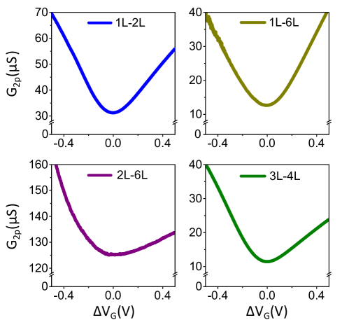
The behaviour observed in 1L-WSe2/1L-SnSe2 interfaces is distinctly different, as illustrated by their two probe conductivity that remains finite for all values of . Fig. 2(e) shows that for negative the conductivity nearly overlaps with the conductivity of the WSe2 monolayer measured on the same device (the structure contains multiple contacts that enable measuring separately the WSe2/SnSe2 interface and the WSe2 layer, see the inset of Fig. 2(e)), it reaches a minimum value of S, and then increases again for positive values. No extended interval of gate voltage is present in which vanishes as observed in WSe2 (see cyan curve in Fig. 2(e)) or in WSe2/ZrS2 interfaces (see Fig. 2(d)). The observed qualitative behavior –expected from a semimetal or a zero-gap semiconductor such as graphene– is robust and was observed in all WSe2/SnSe2 interfaces that we studied, irrespective of the thickness of the constituent layers, as illustrated by the measurements performed on different devices shown in Fig. 3. These observations provide a direct indication of the absence of a sizable band gap in WSe2/SnSe2, confirming the conclusion suggested by the quenching of PL observed in 1L-WSe2/1L-SnSe2 discussed above.
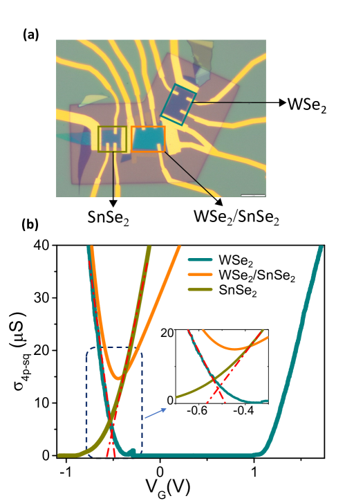
With the aim to probe the electronic properties of WSe2/SnSe2 interfaces more in detail, we fabricated a structure enabling the two constituent layers and their interface to be probed separately with multiterminal measurements done on a same device. The structure consists of two large exfoliated crystals of 3L-WSe2 and a 4L-SnSe2 that are partially stacked on top of each other, in such a way that also the two constituent layers can be contacted (see Fig. 4(a)). For both layers and for the interface the nano-fabricated contacts do not only enable the longitudinal conductivity to be measured, but also the Hall resistance. All parts of the structure are immersed into a droplet of ionic liquid that covers a common gate electrode. To avoid the possibility of material degradation, we took care to cover with a hBN monolayer the part of the SnSe2 layer not covered by WSe2.
FET transfer curves measured on the two individual layers and on their interface are plotted in Fig.4b. The transfer curve of WSe2 (cyan line) exhibits a full gap, as already discussed for the monolayer case (Fig. 2(e); being thicker than a monolayer, the gap in 3L-WSe2 is smaller, as expected). For the SnSe2 part of the device, the transfer curve (olive line) exhibits conventional behavior, with a clear onset for electron transport below which the conductivity vanishes (not being relevant here, we did not apply a negative gate voltage large enough to accumulate holes, to avoid risking device degradation). In line with the behavior shown in Fig. 2(e) and Fig. 3, the interface transfer curve (orange line) exhibits a minimum, with the conductivity remaining finite for all value of . For V, the curve measured on the interface overlaps almost perfectly with the corresponding curve measured on WSe2, showing that in this range of voltages, the interfacial conductivity originates from holes accumulated in WSe2. For V the interfacial conductivity increases upon increasing , and its value remains close to that measured on the SnSe2 part of the device, consistently with the notion that in this gate voltage range interfacial transport is mediated by electrons accumulated in SnSe2. The absolute value of the interface conductivity, however, is slightly smaller than in the individual SnSe2 layer, and so is the slope with which increases for larger positive . The difference is likely due to the capacitance between the liquid and the SnSe2 layer, which is smaller in the interface region, since there the SnSe2 layer is separated from the liquid by a 3L-WSe2, considerably thicker than the monolayer hBN used to protect SnSe2 in the region away from the interface. The data therefore indicate that transport in the interface region is mediated by holes in WSe2 for values sufficiently smaller than V and by electrons in SnSe2 for values sufficiently larger than V, with the conductivity remaining finite for all values in between (i.e., without vanishing over an extended interval as it happens in the presence of a band gap).
At a more quantitative level, in this device we can determine the threshold voltage for electron conduction in the SnSe2 and the threshold voltage for hole conduction in the WSe2, by extrapolating to zero the -dependent conductivity of the respective individual layers (see red dashed-dotted lines in Fig. 4(b)). As explained above, the threshold voltages correspond to having the chemical potential located respectively at the conduction band edge of SnSe2 or at the valence band edge of WSe2. We see in Fig. 4(b) that , allowing us to conclude directly from the experiments that the valence band edge of WSe2 is higher in energy than the conduction band edge of SnSe2, i.e., that the band alignment of the two materials does exhibit a band overlap. The data also provide an estimate of the magnitude of this overlap, given by meV (with a relatively large uncertainty, originating from the extrapolation procedure).
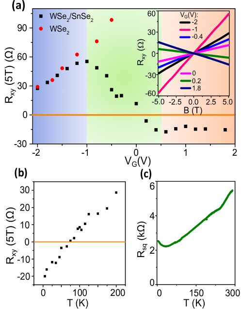
Having concluded that 3L-WSe2/4L-SnSe2 interfaces are indeed semimetals, we search for the expected manifestations of the semimetallic state in their magnetic-field () and temperature () dependent transport properties. We first look at the Hall resistance measured as a function of gate voltage (see black squares in Fig. 5(a)). Starting from large negative values, i.e., when the Fermi level is in the valence band of the interface, the Hall resistance measured at fixed applied magnetic field T (extracted from the curves shown in the inset of Fig. 5(a)) is positive, and initially increases upon shifting to less negative values (corresponding to a decrease in hole density). In this interval the Hall resistance coincides with the one measured on the WSe2 layer (red circles in Fig. 5(a)), confirming that transport in the interface is mediated by states in the valence band of WSe2. Shifting past V, causes the Hall resistance to decrease, because in this interval of gate voltage both holes and electrons are present. Indeed, upon increasing past approximately V, the Hall resistance changes sign and becomes negative. Increasing further on the positive side causes the Hall resistance to decrease only very slowly, likely because of the lower capacitance of the ionic liquid to the SnSe2 layer (as we already mentioned, the ionic liquid is separated from SnSe2 by the 3L-WSe2 that is relatively thick) and because exfoliated SnSe2 layers are unintentionally electron doped (i.e., electrons are naturally present in the material at room temperature even in the absence of any applied gate voltage, see Fig. 4(b)). Irrespective of these details, the overall evolution of the Hall resistance as a function of shows the coexistence in the interface of electrons and holes in an extended range of gate voltages \bibnoteTo avoid any possible ambiguity we remark explicitly that –contrary to the case when the Fermi level is inside the gap of a semiconducting material– if the chemical potential lies within the band overlap region (because the term in Eq.(1) cannot be neglected). That is why the interval over which electron and holes coexist (green shaded region in Fig. 5 (a)) is much larger than 80 meV, i.e., the value of band overlap estimated earlier, which is precisely the behavior expected for a semimetal. The presence of both electrons and holes further manifests itself in the temperature evolution of the Hall resistance, as shown in Fig. 5(b) for the 2L-WSe2/6L-SnSe2 interface whose transfer curve is shown in Fig. 3. Upon lowering the temperature at V, the Hall resistance changes from positive to negative upon cooling, as the dominating contribution to transport changes from being given by holes at high temperature and by electrons at low temperature. This observation confirms that electrons and holes indeed coexist at the interface.
The presence of a semimetallic state is confirmed by looking at the temperature dependence of the longitudinal square resistance () of the WSe2/SnSe2 interfaces. Fig. 5(c) shows the square resistance measured on a 2L-WSe2/6L-SnSe2 interface gate-biased at the conductance minimum. The square resistance decreases from just over 5k at room temperature to approximately 2.5k at K, i.e. interfaces gate-biased at their minimum conductivity exhibit a metallic temperature dependence of their resistivity as expected for a semimetal (despite the fact that the interface is formed by two semiconducting materials). We observed metallic temperature dependence in all our devices on which multi-terminal measurements were performed, including devices in which the -dependent resistivity measurements were performed before placing the ionic-liquid, i.e., on the as-assembled structures. For some structures –including 1L-WSe2/1L-SnSe2 interfaces– we only realized two-terminal devices, not suitable to perform reliable -dependent resistivity measurements, because of the influence of the contact resistance (which can be large depending on the sample). Even if for these interfaces we cannot entirely exclude that a small gap (rather than a band overlap) is present, all measurements from which a firm conclusion can be drawn (i.e., the gate voltage dependence of both the longitudinal and transverse resistance and the temperature dependence of the longitudinal resistance in all multi-terminal devices investigated) systematically indicate the occurrence of a semimetallic state at WSe2/SnSe2 interfaces.
We emphasize that all the transport properties that we observed in WSe2/SnSe2 interfaces –the presence of a finite minimum of conductance, the change of sign of the Hall resistance as a function of both gate voltage and temperature, and the metallic temperature dependence of the longitudinal resistance at the minimum of conductance– are distinctly different from those of the two constituent layers, which are large band gap semiconductors. In the absence of any type of charge accumulation (i.e., due to chemical doping or to a suitably applied gate voltage) WSe2 is an insulator. Even when gate-doped at sufficiently high carrier density to exhibit metallic transport properties, WSe2 never exhibits any signature of spatially coexisting electrons and holes. Similar considerations hold true for SnSe2. Past experiments51 –as well as our work– find that exfoliated SnSe2 layers are unintentionally doped with a rather high density of electrons, and hence show a rather high room-temperature conductivity at = 0V. However, at sufficiently low temperature the square resistance exhibits an exponential increase (shown in Fig. S2(a)). Additionally, as shown in Fig. 4b, gating allows atomically thin SnSe2 layers to be completely depleted, illustrating clearly the presence of a gap. This comparison between the WSe2/SnSe2 interfaces and the individual WSe2 and SnSe2 layers perfectly illustrate the concept of ”synthetic semimetal”: WSe2/SnSe2 vdW interfaces truly are a new system behaving in all regards as a semimetal, despite being formed by two atomically thin crystals that are themselves large-gap semiconductors.
In summary, we have realized interfaces based on atomically thin layers of WSe2 and SnSe2 and shown that they are semimetals. As semimetallic systems can host a variety of interesting physical phenomena depending on microscopic details of their electronic structure, the possibility to study them using vdW interfaces is particularly attractive. Indeed, interfaces offer an experimental control that is not available in naturally occurring semimetals. For instance, the spatial separation of electron and holes –hosted in the two different layers forming the interface– enables the system to be tuned continuously through the application of a perpendicular electric field that shifts the relative electrostatic potential of the two layers, and to control the overlap between valence and conduction band (to either increase it or suppress it). That is why synthetic semimetals based on van der Waals interfaces of the type demonstrated in our work represent an interesting platform with very considerable potential to reveal new physical phenomena.
We gratefully acknowledge A. Ferreira for continuous technical support and H. Henck for his assistance with the preparation of the figures. A.F.M. gratefully acknowledge financial support from the Swiss National Science Foundation and from the EU Graphene Flagship project.
References
- Geim and Grigorieva 2013 Geim, A. K.; Grigorieva, I. V. Van der Waals heterostructures. Nature 2013, 499, 419–425
- Novoselov et al. 2016 Novoselov, K. S.; Mishchenko, A.; Carvalho, A.; Neto, A. H. C. 2D materials and van der Waals heterostructures. Science 2016, 353, aac9439
- Iannaccone et al. 2018 Iannaccone, G.; Bonaccorso, F.; Colombo, L.; Fiori, G. Quantum engineering of transistors based on 2D materials heterostructures. Nature Nanotechnology 2018, 13, 183–191
- Yankowitz et al. 2012 Yankowitz, M.; Xue, J.; Cormode, D.; Sanchez-Yamagishi, J. D.; Watanabe, K.; Taniguchi, T.; Jarillo-Herrero, P.; Jacquod, P.; LeRoy, B. J. Emergence of superlattice Dirac points in graphene on hexagonal boron nitride. Nature Physics 2012, 8, 382–386
- Dean et al. 2013 Dean, C. R.; Wang, L.; Maher, P.; Forsythe, C.; Ghahari, F.; Gao, Y.; Katoch, J.; Ishigami, M.; Moon, P.; Koshino, M. et al. Hofstadter’s butterfly and the fractal quantum Hall effect in moiré superlattices. Nature 2013, 497, 598–602
- Ponomarenko et al. 2013 Ponomarenko, L. A.; Gorbachev, R. V.; Yu, G. L.; Elias, D. C.; Jalil, R.; Patel, A. A.; Mishchenko, A.; Mayorov, A. S.; Woods, C. R.; Wallbank, J. R. et al. Cloning of Dirac fermions in graphene superlattices. Nature 2013, 497, 594–597
- Wang et al. 2015 Wang, Z.; Ki, D.-K.; Chen, H.; Berger, H.; MacDonald, A. H.; Morpurgo, A. F. Strong interface-induced spin–orbit interaction in graphene on . Nature Communications 2015, 6, 1–7
- Wang et al. 2016 Wang, Z.; Ki, D.-K.; Khoo, J. Y.; Mauro, D.; Berger, H.; Levitov, L. S.; Morpurgo, A. F. Origin and Magnitude of ‘Designer’ Spin-Orbit Interaction in Graphene on Semiconducting Transition Metal Dichalcogenides. Physical Review X 2016, 6, 041020
- Benítez et al. 2018 Benítez, L. A.; Sierra, J. F.; Torres, W. S.; Arrighi, A.; Bonell, F.; Costache, M. V.; Valenzuela, S. O. Strongly anisotropic spin relaxation in graphenetransition metal dichalcogenide heterostructures at room temperature. Nature Physics 2018, 14, 303–308
- Island et al. 2019 Island, J. O.; Cui, X.; Lewandowski, C.; Khoo, J. Y.; Spanton, E. M.; Zhou, H.; Rhodes, D.; Hone, J. C.; Taniguchi, T.; Watanabe, K. et al. Spinorbitdriven band inversion in bilayer graphene by the van der Waals proximity effect. Nature 2019, 571, 85–89
- Wang et al. 2019 Wang, D.; Che, S.; Cao, G.; Lyu, R.; Watanabe, K.; Taniguchi, T.; Lau, C. N.; Bockrath, M. Quantum Hall Effect Measurement of SpinOrbit Coupling Strengths in Ultraclean Bilayer Graphene/ Heterostructures. Nano Letters 2019, 19, 7028–7034
- Avsar et al. 2019 Avsar, A.; Ochoa, H.; Guinea, F.; Ozyilmaz, B.; van Wees, B. J.; Vera-Marun, I. J. Colloquium: Spintronics in graphene and other two-dimensional materials. arXiv:1909.09188 2019,
- Cao et al. 2018 Cao, Y.; Fatemi, V.; Fang, S.; Watanabe, K.; Taniguchi, T.; Kaxiras, E.; Jarillo-Herrero, P. Unconventional superconductivity in magic-angle graphene superlattices. Nature 2018, 556, 43–50
- Lu et al. 2019 Lu, X.; Stepanov, P.; Yang, W.; Xie, M.; Aamir, M. A.; Das, I.; Urgell, C.; Watanabe, K.; Taniguchi, T.; Zhang, G. et al. Superconductors, orbital magnets and correlated states in magic-angle bilayer graphene. Nature 2019, 574, 653–657
- Yankowitz et al. 2019 Yankowitz, M.; Chen, S.; Polshyn, H.; Zhang, Y.; Watanabe, K.; Taniguchi, T.; Graf, D.; Young, A. F.; Dean, C. R. Tuning superconductivity in twisted bilayer graphene. Science 2019, 363, 1059–1064
- Codecido et al. 2019 Codecido, E.; Wang, Q.; Koester, R.; Che, S.; Tian, H.; Lv, R.; Tran, S.; Watanabe, K.; Taniguchi, T.; Zhang, F. et al. Correlated insulating and superconducting states in twisted bilayer graphene below the magic angle. Science Advances 2019, 5, eaaw9770
- Wu et al. 2019 Wu, F.; Lovorn, T.; Tutuc, E.; Martin, I.; MacDonald, A. Topological Insulators in Twisted Transition Metal Dichalcogenide Homobilayers. Physical Review Letters 2019, 122, 086402
- Wang et al. 2019 Wang, L.; Shih, E.-M.; Ghiotto, A.; Xian, L.; Rhodes, D. A.; Tan, C.; Claassen, M.; Kennes, D. M.; Bai, Y.; Kim, B. et al. Magic continuum in twisted bilayer . arXiv:1910.12147 2019, 1–8
- Xi et al. 2016 Xi, X.; Wang, Z.; Zhao, W.; Park, J.-H.; Law, K. T.; Berger, H.; Forró, L.; Shan, J.; Mak, K. F. Ising pairing in superconducting NbSe atomic layers. Nature Physics 2016, 12, 139–143
- Sharma et al. 2018 Sharma, C. H.; Surendran, A. P.; Varma, S. S.; Thalakulam, M. 2D superconductivity and vortex dynamics in 1T-. Communications Physics 2018, 1, 1–8
- Gong et al. 2017 Gong, C.; Li, L.; Li, Z.; Ji, H.; Stern, A.; Xia, Y.; Cao, T.; Bao, W.; Wang, C.; Wang, Y. et al. Discovery of intrinsic ferromagnetism in two-dimensional van der Waals crystals. Nature 2017, 546, 265–269
- Huang et al. 2017 Huang, B.; Clark, G.; Navarro-Moratalla, E.; Klein, D. R.; Cheng, R.; Seyler, K. L.; Zhong, D.; Schmidgall, E.; McGuire, M. A.; Cobden, D. H. et al. Layer-dependent ferromagnetism in a van der Waals crystal down to the monolayer limit. Nature 2017, 546, 270–273
- Deng et al. 2018 Deng, Y.; Yu, Y.; Song, Y.; Zhang, J.; Wang, N. Z.; Sun, Z.; Yi, Y.; Wu, Y. Z.; Wu, S.; Zhu, J. et al. Gate-tunable room-temperature ferromagnetism in two-dimensional . Nature 2018, 563, 94–99
- Song et al. 2018 Song, T.; Cai, X.; Tu, M. W.-Y.; Zhang, X.; Huang, B.; Wilson, N. P.; Seyler, K. L.; Zhu, L.; Taniguchi, T.; Watanabe, K. et al. Giant tunneling magnetoresistance in spin-filter van der Waals heterostructures. Science 2018, 360, 1214–1218
- Wang et al. 2018 Wang, Z.; Gutiérrez-Lezama, I.; Ubrig, N.; Kroner, M.; Gibertini, M.; Taniguchi, T.; Watanabe, K.; Imamoğlu, A.; Giannini, E.; Morpurgo, A. F. Very large tunneling magnetoresistance in layered magnetic semiconductor . Nature Communications 2018, 9, 1–8
- Gibertini et al. 2019 Gibertini, M.; Koperski, M.; Morpurgo, A. F.; Novoselov, K. S. Magnetic 2D materials and heterostructures. Nature Nanotechnology 2019, 14, 408–419
- Terashima et al. 2003 Terashima, K.; Sato, T.; Komatsu, H.; Takahashi, T.; Maeda, N.; Hayashi, K. Charge-density wave transition of studied by angle-resolved photoemission spectroscopy. Physical Review B 2003, 68, 155108
- Soumyanarayanan et al. 2013 Soumyanarayanan, A.; Yee, M. M.; He, Y.; Wezel, J. v.; Rahn, D. J.; Rossnagel, K.; Hudson, E. W.; Norman, M. R.; Hoffman, J. E. Quantum phase transition from triangular to stripe charge order in . Proceedings of the National Academy of Sciences 2013, 110, 1623–1627
- Ryu et al. 2018 Ryu, H.; Chen, Y.; Kim, H.; Tsai, H.-Z.; Tang, S.; Jiang, J.; Liou, F.; Kahn, S.; Jia, C.; Omrani, A. A. et al. Persistent Charge-Density-Wave Order in Single-Layer . Nano Lett. 2018, 18, 689–694
- Lee et al. 2014 Lee, C.-H.; Lee, G.-H.; Zande, A. M. v. d.; Chen, W.; Li, Y.; Han, M.; Cui, X.; Arefe, G.; Nuckolls, C.; Heinz, T. F. et al. Atomically thin p–n junctions with van der Waals heterointerfaces. Nature Nanotechnology 2014, 9, 676–681
- Ross et al. 2017 Ross, J. S.; Rivera, P.; Schaibley, J.; Lee-Wong, E.; Yu, H.; Taniguchi, T.; Watanabe, K.; Yan, J.; Mandrus, D.; Cobden, D. et al. Interlayer Exciton Optoelectronics in a 2D Heterostructure p–n Junction. Nano Letters 2017, 17, 638–643
- Ponomarev et al. 2018 Ponomarev, E.; Ubrig, N.; Gutiérrez-Lezama, I.; Berger, H.; Morpurgo, A. F. Semiconducting van der Waals Interfaces as Artificial Semiconductors. Nano Letters 2018, 18, 5146–5152
- Knez et al. 2011 Knez, I.; Du, R.-R.; Sullivan, G. Evidence for Helical Edge Modes in Inverted Quantum Wells. Physical Review Letters 2011, 107, 136603
- Suzuki et al. 2013 Suzuki, K.; Harada, Y.; Onomitsu, K.; Muraki, K. Edge channel transport in the topological insulating phase. Physical Review B 2013, 87, 235311
- Du et al. 2015 Du, L.; Knez, I.; Sullivan, G.; Du, R.-R. Robust Helical Edge Transport in Gated Bilayers. Physical Review Letters 2015, 114, 096802
- Zhu et al. 2011 Zhu, Z. Y.; Cheng, Y. C.; Schwingenschlögl, U. Giant spin-orbit-induced spin splitting in two-dimensional transition-metal dichalcogenide semiconductors. Physical Review B 2011, 84, 153402
- Xiao et al. 2012 Xiao, D.; Liu, G.-B.; Feng, W.; Xu, X.; Yao, W. Coupled Spin and Valley Physics in Monolayers of and Other Group-VI Dichalcogenides. Physical Review Letters 2012, 108, 196802
- Kośmider et al. 2013 Kośmider, K.; González, J. W.; Fernández-Rossier, J. Large spin splitting in the conduction band of transition metal dichalcogenide monolayers. Physical Review B 2013, 88, 245436
- Jérome et al. 1967 Jérome, D.; Rice, T. M.; Kohn, W. Excitonic Insulator. Physical Review 1967, 158, 462–475
- Zhang et al. 2016 Zhang, C.; Gong, C.; Nie, Y.; Min, K.-A.; Liang, C.; Oh, Y. J.; Zhang, H.; Wang, W.; Hong, S.; Colombo, L. et al. Systematic study of electronic structure and band alignment of monolayer transition metal dichalcogenides in Van der Waals heterostructures. 2D Materials 2016, 4, 015026
- Koda et al. 2018 Koda, D. S.; Bechstedt, F.; Marques, M.; Teles, L. K. Trends on band alignments: Validity of Anderson’s rule in - and -based van der Waals heterostructures. Physical Review B 2018, 97, 165402
- Kashiwabara et al. 2019 Kashiwabara, Y.; Nakano, M.; Nakagawa, Y.; Wang, Y.; Matsuoka, H.; Iwasa, Y. Electrical Conduction at the Interface between Insulating van der Waals Materials. Advanced Functional Materials 2019, 29, 1900354
- Braga et al. 2012 Braga, D.; Gutiérrez Lezama, I.; Berger, H.; Morpurgo, A. F. Quantitative Determination of the Band Gap of with Ambipolar Ionic Liquid-Gated Transistors. Nano Letters 2012, 12, 5218–5223
- Lezama et al. 2014 Lezama, I. G.; Ubaldini, A.; Longobardi, M.; Giannini, E.; Renner, C.; Kuzmenko, A. B.; Morpurgo, A. F. Surface transport and band gap structure of exfoliated 2H- crystals. 2D Materials 2014, 1, 021002
- Jo et al. 2014 Jo, S.; Ubrig, N.; Berger, H.; Kuzmenko, A. B.; Morpurgo, A. F. Mono- and Bilayer Light-Emitting Transistors. Nano Letters 2014, 14, 2019–2025
- Gutiérrez-Lezama et al. 2016 Gutiérrez-Lezama, I.; Reddy, B. A.; Ubrig, N.; Morpurgo, A. F. Electroluminescence from indirect band gap semiconductor . 2D Materials 2016, 3, 045016
- Zhang et al. 2019 Zhang, H.; Berthod, C.; Berger, H.; Giamarchi, T.; Morpurgo, A. F. Band Filling and Cross Quantum Capacitance in Ion-Gated Semiconducting Transition Metal Dichalcogenide Monolayers. Nano Letters 2019, 19, 8836–8845
- Ponomarev et al. 2015 Ponomarev, E.; Gutiérrez-Lezama, I.; Ubrig, N.; Morpurgo, A. F. Ambipolar Light-Emitting Transistors on Chemical Vapor Deposited Monolayer . Nano Letters 2015, 15, 8289–8294
- Ponomarev et al. 2018 Ponomarev, E.; Pásztor, A.; Waelchli, A.; Scarfato, A.; Ubrig, N.; Renner, C.; Morpurgo, A. F. Hole Transport in Exfoliated Monolayer . ACS Nano 2018, 12, 2669–2676
- 50 To avoid any possible ambiguity we remark explicitly that –contrary to the case when the Fermi level is inside the gap of a semiconducting material– if the chemical potential lies within the band overlap region (because the term in Eq.(1) cannot be neglected). That is why the interval over which electron and holes coexist (green shaded region in Fig. 5 (a)) is much larger than 80 meV, i.e., the value of band overlap estimated earlier
- Zeng et al. 2018 Zeng, J.; Liu, E.; Fu, Y.; Chen, Z.; Pan, C.; Wang, C.; Wang, M.; Wang, Y.; Xu, K.; Cai, S. et al. Gate-Induced Interfacial Superconductivity in 1T-. Nano Letters 2018, 18, 1410–1415