Single Spin Localization and Manipulation
in Graphene Open-Shell Nanostructures
Abstract
Predictions state that graphene can spontaneously develop magnetism from the Coulomb repulsion of its -electrons, but its experimental verification has been a challenge. Here, we report on the observation and manipulation of individual magnetic moments localized in graphene nanostructures on a Au(111) surface. Using scanning tunneling spectroscopy, we detected the presence of single electron spins localized around certain zigzag sites of the carbon backbone via the Kondo effect. Two near-by spins were found coupled into a singlet ground state, and the strength of their exchange interaction was measured via singlet-triplet inelastic tunnel electron excitations. Theoretical simulations demonstrate that electron correlations result in spin-polarized radical states with the experimentally observed spatial distributions. Hydrogen atoms bound to these radical sites quench their magnetic moment, permitting us to switch the spin of the nanostructure using the tip of the microscope.
Among the many applications predicted for graphene, its use as a source of magnetism is the most unexpected one, and an attractive challenge for its active role in spintronic devices [1]. Generally, magnetism is associated to a large degree of electron localization and strong spin-orbit interaction. Both premises are absent in graphene, a strongly diamagnetic material. The simplest method to induce magnetism in graphene is to create an imbalance in the number of carbon atoms in each of the two sublattices, what, according to the Lieb’s theorem for bipartite lattices [2], causes a spin imbalance in the system. This can be done by either inserting defects that remove a single orbital [3, 4, 5, 6] or by shaping graphene with zigzag edges [7, 8]. However, magnetism can also emerge in graphene nanostructures where Lieb’s theorem does not apply [9, 10]. For example, in -conjugated systems with small band gaps, Coulomb repulsion between valence electrons forces the electronic system to reorganize into open-shell configurations [11] with unpaired electrons (radicals) localized at different atomic sites. Although the net magnetization of the nanostructures may be zero, each radical state hosts a magnetic moment of size , the Bohr magneton, turning the graphene nanostructure paramagnetic. This basic principle predicts, for example, the emergence of edge magnetization originating from zero-energy modes in sufficiently wide zigzag [12, 13, 14] and chiral [15, 16] graphene nanoribbons (GNRs).
The experimental observation of spontaneous magnetization driven by electron correlations is still challenging, because, for example, atomic defects and impurities in the graphene structures [17, 18] hide the weak paramagnetism of radical sites [19]. Scanning probe microscopies can spatially localize the source states of magnetism, but they require both atomic-scale resolution and spin-sensitive measurements. Here we achieve these conditions to demonstrate that atomically-defined graphene nanostructures can host localized spins at specific sites and give rise to the Kondo effect [20, 21], a many-body phenomenon caused by the interaction between a localized spin and free conduction electrons in its proximity. Using a low-temperature scanning tunneling microscope (STM) we use this signal to map the spin localization within the nanostructure and to detect spin-spin interactions.
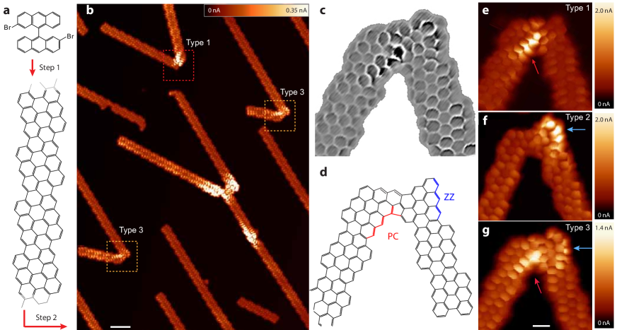
The graphene nanostructures studied here are directly created on a Au(111) surface by cross-dehydrogenative coupling of adjacent chiral GNRs (chGNRs)[22]. We deposited the organic molecular precursors 2,2’-dibromo-9,9’-bianthracene (Fig. 1a) on a clean Au(111) surface, and annealed stepwisely to 250 ∘C (step 1 in Fig. 1a) to produce narrow chGNRs[14, 23]. The chiral ribbons are semiconductors with a band-gap of 0.7 eV (Supplementary Figs. S7 and S8) and show two enantiomeric forms on the surface[24]. By further annealing the substrate to 350 ∘C (step 2 in Fig. 1a), chGNRs fuse together into junctions, as shown in Fig. 1b. The chGNR junctions highlighted by dashed rectangles are the most frequently found in our experiments. They consist of two chGNRs with the same chirality linked together by their termination (Fig. 1c). The creation of this stable nanostructure implies the reorganization of the carbon atoms around the initial contact point[25] into the final structure shown in Fig. 1d, as described in Supplementary Fig. S1.
In Fig. 1b, certain regions of the junctions appear brighter when recorded at low sample bias, reflecting enhancements of the local density of states (LDOS) close to the Fermi level. Interestingly, the precise location of the bright regions is not unique, but can be localized over the pentagon cove (PC) site (Type 1, Fig. 1e), over the terminal zigzag (ZZ) site of the junction (Type 2, Fig. 1f), or over both (Type 3, Fig. 1g). Despite these different LDOS distributions in the three types of junctions, they have identical carbon arrangement (Fig. 1d).
To understand the origin of the enhanced LDOS at the ZZ and PC sites, we recorded differential conductance spectra () on the three types of junctions. Spectra on the bright sites of Type 1 and 2 junctions show very pronounced zero-bias peaks (Fig. 2a,b) localized over the bright sites (spectra 1 to 4, and 6 to 8), and vanishing rapidly in neighbor rings (spectra 5, 9, and 10). These are generally ascribed as Abrikosov-Suhl resonances due to the Kondo effect, and named as Kondo resonances[20, 21]. Their observation is a proof of a localized magnetic moment screened by conduction electrons[26, 27]. The resonance line width increases with temperature (Fig. 2d) and magnetic field (Fig. 2e) following the characteristic behavior of a spin-½ system with a Kondo Temperature K[28, 27].
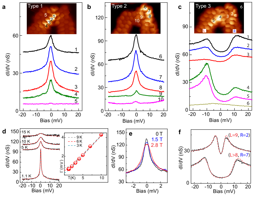
Junctions with two bright regions (Type 3) show different low-energy features: two peaked steps in spectra at 10 meV (Fig. 2c). The peaks appear at the same energies over the terminal ZZ segment and over the PC region for a given nanostructure, and vanish quickly away from these sites. Based on the existence of localized spins on bright areas of Type 1 and 2 junctions, we attribute the double-peak features to excitation of two exchange coupled spins localized at each junction site. The exchange interaction tends to freeze their relative orientation, in this case antiferromagnetically into a singlet ground state. Electrons tunneling into the coupled spin system can excite a spin reversal in any of them when their energy equals the exchange coupling energy between the spins, i.e., . Usually, this inelastic process is revealed in spectra as steps at the onset of spin excitations[31], from which one can directly determine the strength of the exchange coupling between the spins. Here, the spectra additionally show asymmetric peaks on top of the excitation onsets characteristic of Kondo-like systems with particle-hole asymmetry, when spin fluctuations are hindered in the ground state[32, 33, 30, 34]. Hence, the gap between peaks in Fig. 2c is a measure of the interaction strength between the two localized spins.
Interestingly, the spectral gap in Type 3 junctions increases with the length of the connecting ribbons (See Supplementary Fig. 15b). In Fig. 2f we compare low-energy spectra of two junctions with different chGNR lengths. Although the atomic structures of both junctions are identical, the one with shorter ribbons (upper curve; 9 and 2 precursor units) displays a smaller gap than the junction of longer chGNRs (lower curve; and 7 units). Fitting the spectra with a model of two coupled spin-½ systems[30], one obtains the exchange coupling () meV for the upper (lower) spectrum.
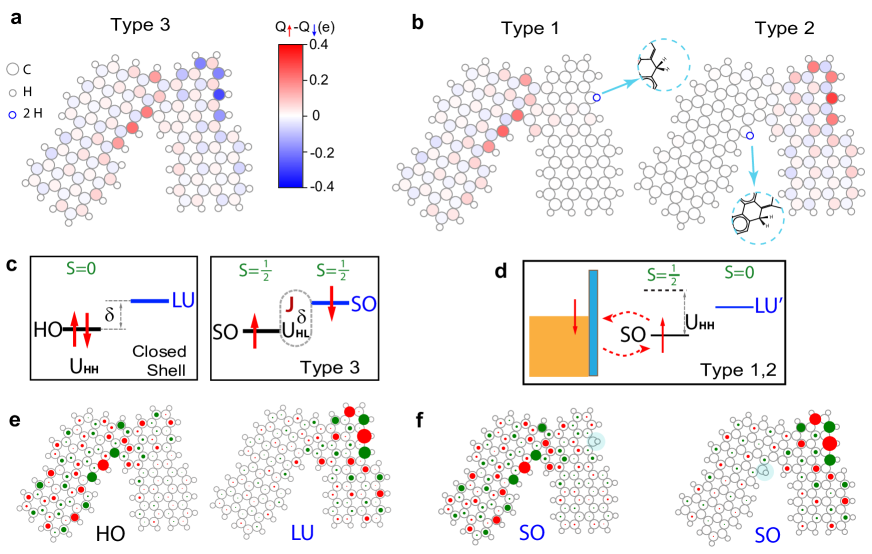
To explain the emergence of localized spins, we simulated the spin-polarized electronic structure of chGNR junctions using both density functional theory (DFT) and mean-field Hubbard (MFH) models (see Supplementary Sections 5 and 6). Fig. 3a shows the spin-polarization of a junction of Fig. 1d. The ground state exhibits a net spin localization at the ZZ and PC regions with opposite sign, which is absent in the bare ribbons. This spin distribution agrees with the observations for Type 3 junctions. The origin of the spontaneous magnetization can be rationalized by considering the effect of Coulomb correlations between -electrons as described within a tight-binding (TB) model. The spin distribution is related to the appearance of two junction states inside the gap of the (3,1)-chGNR electronic bands, localized at the PC and ZZ sites, respectively. In the absence of electron-electron correlations, these two states conform the highest occupied (HO) and lowest unoccupied (LU) molecular states of the nanostructure (Fig. 3e). Due to the large degree of localization (Supplementary Figs. S10-S11), the Coulomb repulsion energy between two electrons in the HO state becomes comparable with the energy difference between the two localized levels. Hence, in a simplified picture, the two electrons find a lower-energy configuration by occupying each a different, spatially separated in-gap state. These two states become singly occupied (SO), spin-polarized (i.e., they have a net magnetic moment), and exchange coupled as schematically illustrated in Fig. 3c. Similar conclusions regarding the emergence of radical states at PC and ZZ sites can also be reached using the empirical Clar’s aromatic -sextet rule (Supplementary Section 3).
According to both DFT (Fig. 3a) and MFH (Supplementary Fig. S9) the magnetic moments are antiferromagnetically aligned into a singlet ground state. Therefore, the inelastic features in spectra found over Type 3 junctions (Fig. 2c) are associated to singlet-triplet excitations induced by tunneling electrons. In fact, the smaller excitation energy found for the smaller ribbons in both theory and experiment (Supplementary Section 7) agrees with a weaker exchange interaction due to a larger localization of the spin-polarized states. Alternative scenarios for peaks around , such as single-particle states or Coulomb-split radical states[6], would show the opposite trend with the system size.
To account for spin localization in only one of the two radical regions in Type 1 and 2 junctions, one of the two edge magnetic moments has to vanish. H-passivation of radical sites is a highly probable process occurring on the surface due to the large amount of hydrogen available during the reaction[35]. DFT simulations show that attaching an extra H atom into an edge carbon in either the ZZ (Type 1) or PC (Type 2) sites leads to its hybridization and the removal of a orbital from the aromatic backbone. This completely quenches the magnetic moment of the passivated region, and leaves the junction with a single electron localized at the opposite radical site (Supplementary Fig. S6). The computed distributions for the two energetically most favorable adsorption sites (Fig. 3b) are in excellent agreement with the extension of the Kondo resonance mapped in Fig. 2a,b.
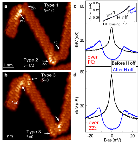
The presence of extra H atoms in Type 1 and 2 junctions was confirmed by electron induced H-atom removal experiments. Figure 4 a shows a structure formed by three chGNRs connected via Type 1 and 2 junctions. Accordingly, their spectra (black curves in Figs. 4c,d) show a Kondo resonance at the PC1 and ZZ2 regions. We placed the STM tip on top of the opposite sites ZZ1 and PC2, and raised the positive sample bias well above 1 V. A step-wise decrease of the tunneling current indicated the removal of the extra H atom (inset in Fig. 4c). The resulting junction appeared with double bright regions in low-bias images (Fig. 4b), and the PC1 and ZZ2 spectra turned into dI/dV steps characteristic of Type 3 junctions (blue curves in Figs. 4c,d). Thus, the removal of H atoms activated the magnetic moment of the initially unpolarized ZZ1 and PC2 sites, converting Type 1 and 2 junctions into Type 3, and switching the total spin of the junction from spin ½ to zero.
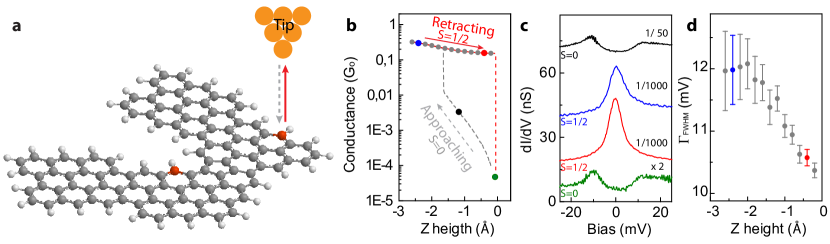
The magnetic state of the junction was also changed by creating a contact between the STM tip apex and a radical site. In the experiments shown in Figure 5, the STM tip was approached to the ZZ sites of a Type 3 junction. A step in the conductance-distance plot (Fig. 5b) indicated the formation of a contact. The created tip-chGNR contact could be stretched up to 3 Å before breaking (retraction step in Fig. 5b), signaling that a chemical bond was formed. spectra recorded before the bond formation (black point in Fig. 5c) shows the split-peak feature of Type 3 junctions (black spectrum in Fig. 5c). After the bond formation (blue and red points in Fig. 5b), the spectra changed to show Kondo resonances (blue and red spectra in Fig. 5c), persisting during contact retraction until the bond-breaking step, where double-peak features are recovered (green spectrum in Fig. 5c). The formation of a tip-chGNR bond thus removed the spin of the ZZ site, and the transport spectra reflect the Kondo effect due to the remaining spin embedded in the junction. If the STM tip contacts instead the ZZ radical site of a Type 2 junction (shown in Supplementary Section 4) the initial Kondo resonance disappears from the spectra, signaling the complete demagnetization of the junction. The width of the Kondo resonance in the contacted junctions (blue and red plots in Fig. 5c) is significantly larger than in Type 1 and 2 cases, probably because it incorporates scattering with tip states[36, 37], and monotonously narrows as the contact is pulled apart (Fig. 5d). The survival of the Kondo effect in the contacted Type 3 junctions is a remarkable outcome of our experiments, which demonstrate the addressability of such localized magnetic moments in graphene nanostructure devices.
Reference
References
- [1] Han, W., Kawakami, R. K., Gmitra, M. & Fabian, J. Graphene spintronics. Nat. Nanotechnol. 9, 794–807 (2014).
- [2] Lieb, E. H. Two theorems on the hubbard model. Phys. Rev. Lett. 62, 1201 (1989).
- [3] Yazyev, O. V. & Helm, L. Defect-induced magnetism in graphene. Phys. Rev. B 75, 125408 (2007).
- [4] Nair, R. R. et al. Spin-half paramagnetism in graphene induced by point defects. Nat. Phys. 8, 199–202 (2012).
- [5] McCreary, K. M., Swartz, A. G., Han, W., Fabian, J. & Kawakami, R. K. Magnetic Moment Formation in Graphene Detected by Scattering of Pure Spin Currents. Phys. Rev. Lett. 109, 186604 (2012).
- [6] Gonzalez-Herrero, H. et al. Atomic-scale control of graphene magnetism by using hydrogen atoms. Science 352, 437–441 (2016).
- [7] Fernández-Rossier, J. & Palacios, J. J. Magnetism in Graphene Nanoislands. Phys. Rev. Lett. 99, 177204 (2007).
- [8] Yazyev, O. V. Emergence of magnetism in graphene materials and nanostructures. Rep. Prog. Phys. 73, 056501 (2010).
- [9] Alexandre, S. S., Lúcio, A. D., Castro Neto, A. H. & Nunes, R. W. Correlated magnetic states in extended one-dimensional defects in graphene. Nano Lett. 12, 5097–5102 (2012).
- [10] Ortiz, R., Lado, J. L., Melle-Franco, M. & Fernández-Rossier, J. Engineering spin exchange in nonbipartite graphene zigzag edges. Phys. Rev. B 94, 094414 (2016).
- [11] Morita, Y., Suzuki, S., Sato, K. & Takui, T. Synthetic organic spin chemistry for structurally well-defined open-shell graphene fragments. Nat. Chem. 3, 197–204 (2011).
- [12] Son, Y.-W., Cohen, M. L. & Louie, S. G. Half-Metallic Graphene Nanoribbons. Nature 444, 347–350 (2006).
- [13] Tao, C. et al. Spatially Resolving Spin-split Edge States of Chiral Graphene Nanoribbons. Nat. Phys. 7, 616–620 (2011).
- [14] Ruffieux, P. et al. On-surface synthesis of graphene nanoribbons with zigzag edge topology. Nature 531, 489–492 (2016).
- [15] Yazyev, O. V., Capaz, R. B. & Louie, S. G. Theory of magnetic edge states in chiral graphene nanoribbons. Phys. Rev. B 84, 115406 (2011).
- [16] Carvalho, A. R., Warnes, J. H. & Lewenkopf, C. H. Edge magnetization and local density of states in chiral graphene nanoribbons. Phys. Rev. B 89, 245444 (2014).
- [17] Sepioni, M. et al. Limits on intrinsic magnetism in graphene. Phys. Rev. Lett. 105, 207205 (2010).
- [18] Nair, R. R. et al. Dual origin of defect magnetism in graphene and its reversible switching by molecular doping. Nat. Commun. 4, 1–6 (2013).
- [19] Červenka, J., Katsnelson, M. I. & Flipse, C. F. J. Room-temperature ferromagnetism in graphite driven by two-dimensional networks of pointdefects. Nat. Phys. 5, 840–844 (2009).
- [20] Kondo, J. Resistance Minimum in Dilute Magnetic Alloys. Prog. Theor. Phys. 32, 37–49 (1964).
- [21] Ternes, M., Heinrich, A. J. & Schneider, W.-D. Spectroscopic manifestations of the Kondo effect on single adatoms. J. Phys.: Condens. Matter 21, 053001 (2009).
- [22] Dienel, T. et al. Resolving Atomic Connectivity in Graphene Nanostructure Junctions. Nano Lett. 15, 5185–5190 (2015).
- [23] de Oteyza, D. G. et al. Substrate-independent growth of atomically precise chiral graphene nanoribbons. ACS Nano 10, 9000–9008 (2016).
- [24] Merino-Díez, N. et al. Unraveling the electronic structure of narrow atomically precise chiral graphene nanoribbons. J. Phys. Chem. Lett. 9, 25–30 (2018).
- [25] Shiotari, A. et al. Strain-induced skeletal rearrangement of a polycyclic aromatic hydrocarbon on a copper surface. Nat. Commun. 8, 16089 (2017).
- [26] Fernández-Torrente, I., Franke, K. J. & Pascual, J. I. Vibrational Kondo Effect in Pure Organic Charge-Transfer Assemblies. Phys. Rev. Lett. 101, 217203 (2008).
- [27] Zhang, Y.-h. et al. Temperature and magnetic field dependence of a kondo system in the weak coupling regime. Nat. Commun. 4, 2110 (2013).
- [28] Nagaoka, K., Jamneala, T., Grobis, M. & Crommie, M. F. Temperature Dependence of a Single Kondo Impurity. Phys. Rev. Lett. 88, 77205 (2002).
- [29] Frota, H. O. Shape of the Kondo resonance. Phys. Rev. B 45, 1096–1099 (1992).
- [30] Ternes, M. Spin excitations and correlations in scanning tunneling spectroscopy. New J. Phys. 17, 63016 (2015).
- [31] Hirjibehedin, C. F., Lutz, C. P. & Heinrich, A. J. Spin coupling in engineered atomic structures. Science 312, 1021–1024 (2006).
- [32] Heersche, H. B. et al. Kondo effect in the presence of magnetic impurities. Phys. Rev. Lett. 96, 017205 (2006).
- [33] Paaske, J. et al. Non-equilibrium singlet-triplet kondo effect in carbon nanotubes. Nat. Phys. 2, 460–464 (2006).
- [34] Ortiz, R., García-Martínez, N. A., Lado, J. L. & Fernández-Rossier, J. Electrical spin manipulation in graphene nanostructures. arXiv:1712.97282v1 .
- [35] Talirz, L. et al. Termini of Bottom-Up Fabricated Graphene Nanoribbons. J. Am. Chem. Soc. 135, 2060–2063 (2013).
- [36] Jasper-Tönnies, T. et al. Conductance of a Freestanding Conjugated Molecular Wire. Phys. Rev. Lett. 119, 066801 (2017).
- [37] Choi, D.-J., Abufager, P., Limot, L. & Lorente, N. From tunneling to contact in a magnetic atom: The non-equilibrium kondo effect. J. Chem. Phys. 146, 092309 (2017).
- [38] Soler, J. M. et al. The siesta method for ab initio order-n materials simulation. J. Phys.: Condens. Matter 14, 2745–2779 (2002).
- [39] Ceperley, D. M. & Alder, B. J. Ground state of the electron gas by a stochastic method. Phys. Rev. Lett. 45, 566–569 (1980).
- [40] Perdew, J. P., Burke, K. & Ernzerhof, M. Generalized gradient approximation made simple. Phys. Rev. Lett. 77, 3865–3868 (1996).
- [41] Hancock, Y., Uppstu, A., Saloriutta, K., Harju, A. & Puska, M. J. Generalized tight-binding transport model for graphene nanoribbon-based systems. Phys. Rev. B 81, 245402 (2010).
0.1 Sample preparation and experimental details.
The experiments were performed on two different scanning tunneling microscopes
(STM) operating in ultra-high vacuum. A commercial JT STM (from specs) operated
at 1.2 K with a magnetic field up to 3 Tesla was used to measure the temperature
and magnetic field dependence of the Kondo resonance, while other experiments
were done with a home made STM operating at 5 K. Both setups allow in situ
sample preparation and transfer into the STM. The Au(111)
substrate was cleaned in UHV by repeated cycles of Ne+ ion sputtering and
subsequent annealing to 730 K. The molecular
precursor (2,2’-dibromo-9,9’-bianthracene) was sublimated at 170 ∘C
from a Knudsen cell onto the clean Au(111) substrate kept at room temperature.
Then the sample was first annealed at 200 ∘C for 15 minutes in order to
induce the polymerization of the molecular precursors by Ullmann coupling, then
the sample was annealed at 250 ∘C for 5 minutes to trigger the
cyclodehydrogenation to form chiral graphene nanoribbons (chGNRs). A last step
annealing at 350 ∘C for 1 minute created nanostructure junctions.
A tungsten tip functionalized with a CO molecule was used for high resolution
images. All the images in the manuscript were acquired in constant height mode, at
very small voltages, and junction resistances of typically 20 M. The
signal was recorded using a lock-in amplifier with a bias modulation of
mV at 760 Hz.
0.2 Simulations.
We performed calculations with the SIESTA implementation[38] of density functional theory (DFT). Exchange and correlation (XC) were included within either the local (spin) density approximation (LDA)[39] or the generalized gradient approximation (GGA)[40]. We used a 400 Ry cutoff for the real-space grid integrations and a double-zeta plus polarization (DZP) basis set generated with an 0.02 Ry energy shift for the cutoff radii. The molecules, represented with periodic unit cells, were separated by a vacuum of at least 10 Å in any direction. The electronic density was converged to a stringent criterion of . The force tolerance was set to 0.002 eV/Å. Here is a description of a specific method used. To complement the DFT simulations described above we also performed simulations based on the mean-field Hubbard (MFH) model, known to provide a good description for carbon -electron systems[7, 8, 15, 16, 41].
We thank Manuel Vilas-Varela for the synthesis of the chGNR molecular precursor. We are indebted to Carmen Rubio, Dimas G. de Oteyza, Nestor Merino, Nicolás Lorente, Aran García Lekue, and Daniel Sánchez Portal for fruitful discussions.
We acknowledge financial support from Spanish AEI
(MAT2016-78293-C6, FIS2017-83780-P, and the Maria de Maeztu Units of Excellence Programme
MDM-2016-0618), the Basque Government (Dep. Industry, Grant PI-2015-1-42), the EU project
PAMS (610446), the Xunta de Galicia (Centro singular de investigación de Galicia
accreditation 2016-2019, ED431G/09), and the European Regional Development Fund (ERDF).
J.L, and J.I.P. devised the experiment. D.P. designed the
organic synthesis of the chGNR molecular precursor. J.L. realized the measurements. S.S.
and T.F. did the theoretical simulations. All the authors discussed the results.
J.L., T.F., and J.I.P. wrote the manuscript.
The authors declare that they have no competing financial interests.